Light-emitting device

Inactive Publication Date: 2008-11-13
HITACHI CABLE
View PDF2 Cites 16 Cited by
  • Summary
  • Abstract
  • Description
  • Claims
  • Application Information

AI Technical Summary

Benefits of technology

[0011]In view of the foregoing and other exemplary problems, drawbacks, and disadvantages of the conventional methods and structures, an exemplary feature of the present invention is to provide a light-emitting device which increases a light extraction efficiency while an emission intensity and a variation of a wavelength depending on a radiation angle are controlled.

Problems solved by technology

However, when the structure is applied to a light-emitting diode, some problems occur.
Secondly, the light-emitting diode has a light radiation angle much wider than that of a laser.
Secondly, a light-emitting spectrum varies depending on a radiation angle of the light-emitting diode.

Method used


Image

  • Light-emitting device
  • Light-emitting device
  • Light-emitting device

Examples


exemplary embodiment 1

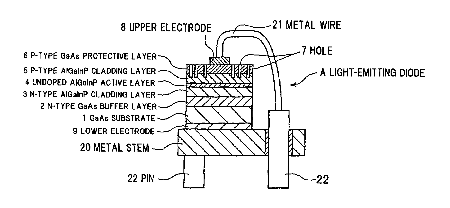
[0033]Hereinafter, a light-emitting diode in an exemplary embodiment according to the present invention is described with reference to the drawings.

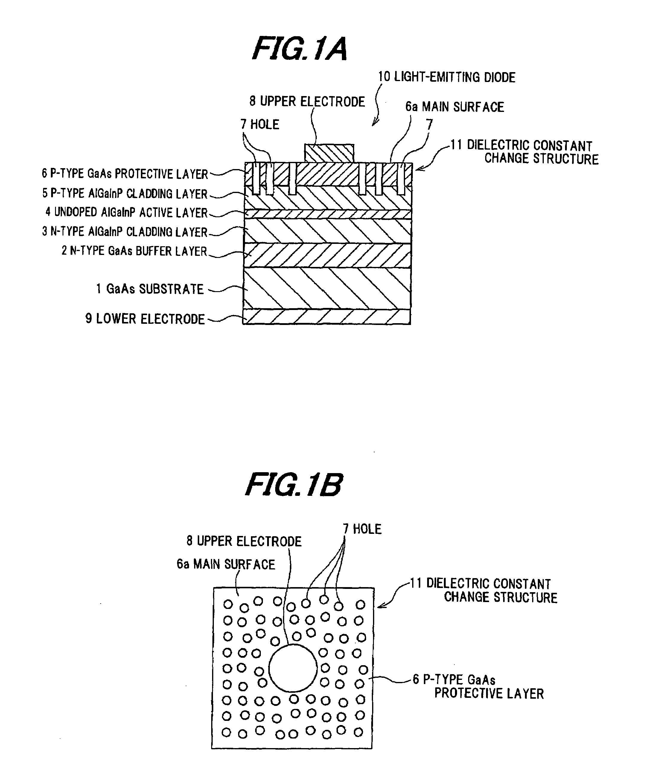
[0034]FIGS. 1A and 1B show a light-emitting diode 10 (bare chip) in an exemplary embodiment according to the present invention. FIG. 1A is a longitudinal sectional view, and FIG. 1B is a top view.

[0035]For making the light-emitting diode 10, an n-type GaAs buffer layer 2, an n-type AlGaInP cladding layer 3, an undoped AlGaInP active layer 4, a p-type AlGaInP cladding layer 5, and a p-type GaAs protective layer 6 are disposed on an n-type GaAs substrate 1 by metalorganic vapor phase epitaxy (MOVPE) in order, and an epitaxial wafer for the light-emitting diode is made.

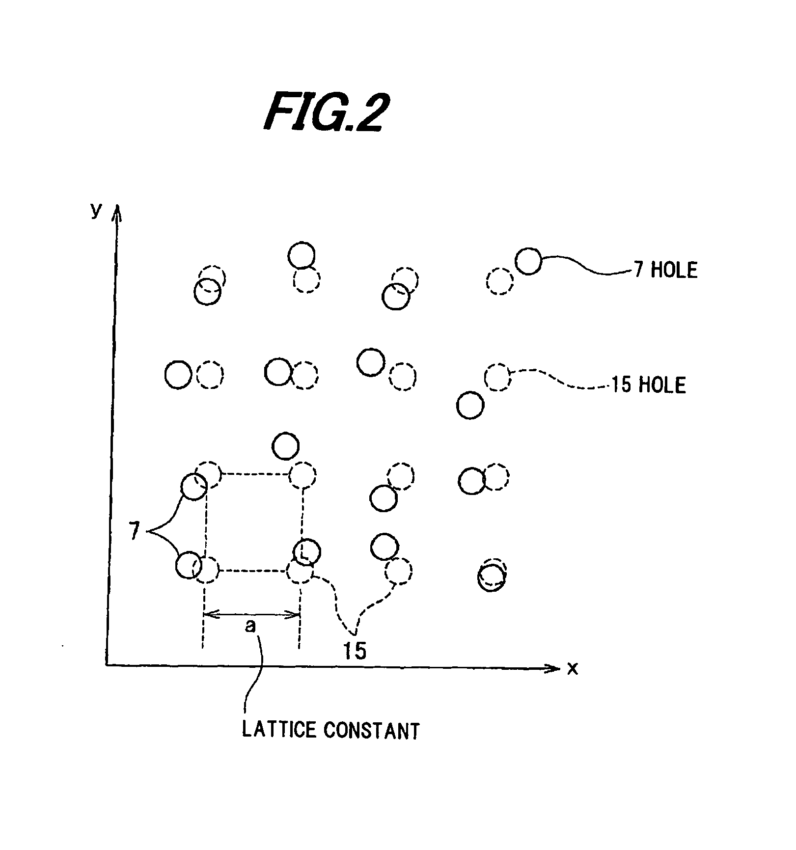
[0036]Next, the p-type GaAs protective layer 6 of the epitaxial wafer is pierced from a surface of the p-type GaAs protective layer 6 as a light extraction surface by photolithography equipment and reactive ion etching (RIE) equipment, and multiple cylindrical holes 7 which r...

example 1

[0055]Next, a light-emitting diode of an example of the present invention is described.

[0056]The light-emitting diode in the example according to the present invention is shown in FIGS. 3A and 3B. FIG. 3A is a longitudinal sectional view showing the light-emitting diode mounted on a stem, and FIG. 3B is a top view showing the light-emitting diode (bare chip) mounted on the stem.

[0057]Firstly, an epitaxial wafer for the light-emitting diode is made just like the above exemplary embodiment. An Si-doped n-type GaAs substrate (circular wafer) 1, a thickness of which may be 300 μm, is mounted on a metalorganic vapor phase epitaxy equipment, and heated up. A group III metalorganic material gas, a group V material gas, and a necessary dopant material gas with a hydrogen carrier gas are supplied to the n-type GaAs substrate 1. An Se-doped n-type GaAs buffer layer 2, a Se-doped n-type (Al0.7Ga0.3)0.5In0.5P cladding layer 3, an undoped (Al0.15Ga0.85)0.5In0.5P active layer 4, a Zn-doped p-type...


PUM


Abstract

A light-emitting device, including a compound semiconductor layer disposed on a substrate, includes a light-emitting layer, and a dielectric constant change structure formed in a part of the compound semiconductor layer including a main surface as a light extraction surface of the compound semiconductor layer. The dielectric constant change structure is devoid of revolution symmetry provided by randomly changing a periodicity of a dielectric constant in a two-dimensional lattice pattern, with respect to a photonic crystal structure in which more than two kinds of materials having different dielectric constants are periodically and alternately disposed on the main surface in the two-dimensional lattice pattern.

Description

[0001]The present application is based on Japanese Patent Application No. 2007-126676 filed on May 11, 2007, the entire contents of which are incorporated herein by reference.BACKGROUND OF THE INVENTION[0002]1. Field of the Invention[0003]This invention relates to a light-emitting device including a light-emitting layer made of a compound semiconductor. More specifically, the light-emitting device is for increasing a light extraction efficiency while a variation of an emission intensity and a wavelength depending on a radiation angle are controlled. The light-emitting device according to the present invention can be used for a device such as a lighting appliance, a backlight for a liquid crystal display (LCD), various types of indicator, a display panel, and the like.[0004]2. Description of the Related Art[0005]In recent years, as applications of a light-emitting diode (LED) increase, a demand for an increased optical output also has increased.[0006]Concerning the demand, a way that...

Claims


Application Information

Patent Timeline
IPC IPC(8): H01L33/00H01L33/22H01L33/30
CPCH01L33/20H01L2224/48137H01L2224/4823H01L2924/01025H01L2933/0083
Inventor AKIMOTO, KATSUYA
Owner HITACHI CABLE
Why Eureka
Try Eureka