

Semiconductor light-emitting device
- Summary
- Abstract
- Description
- Claims
- Application Information
AI Technical Summary
Benefits of technology
Problems solved by technology
Method used
Image

Examples
embodiment 1
1. Semiconductor Light-Emitting Device
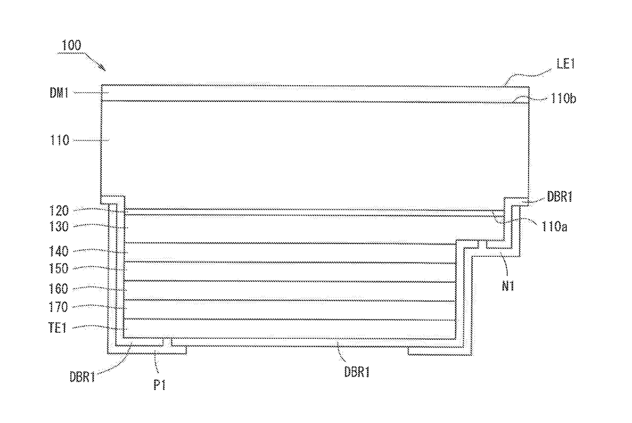
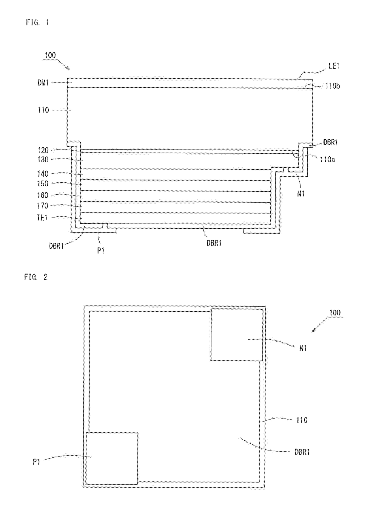
[0038]FIG. 1 is a schematic view of the structure of a light-emitting device 100 according to Embodiment 1. The light-emitting device 100 is a flip-chip type semiconductor light-emitting device having a light extraction surface on the opposite side of a semiconductor layer when viewed from a substrate. As shown in FIG. 1, the light-emitting device 100 includes a dielectric multilayer film DM1, a substrate 110, a buffer layer 120, an n-type contact layer 130, an n-side cladding layer 140, a light-emitting layer 150, a p-side cladding layer 160, a p-type contact layer 170, a transparent electrode TE1, a distributed bragg reflector DBR1, a p-electrode P1, and an n-electrode N1.
[0039]The substrate 110 is a sapphire substrate for transmitting a light emitted from the light-emitting layer 150 to the opposite side of the semiconductor layer. The substrate 110 has a rectangular parallelopiped shape. The substrate 110 has a first surface 110a and a secon...
examples
1. Experiment
1-1. Production of Sample
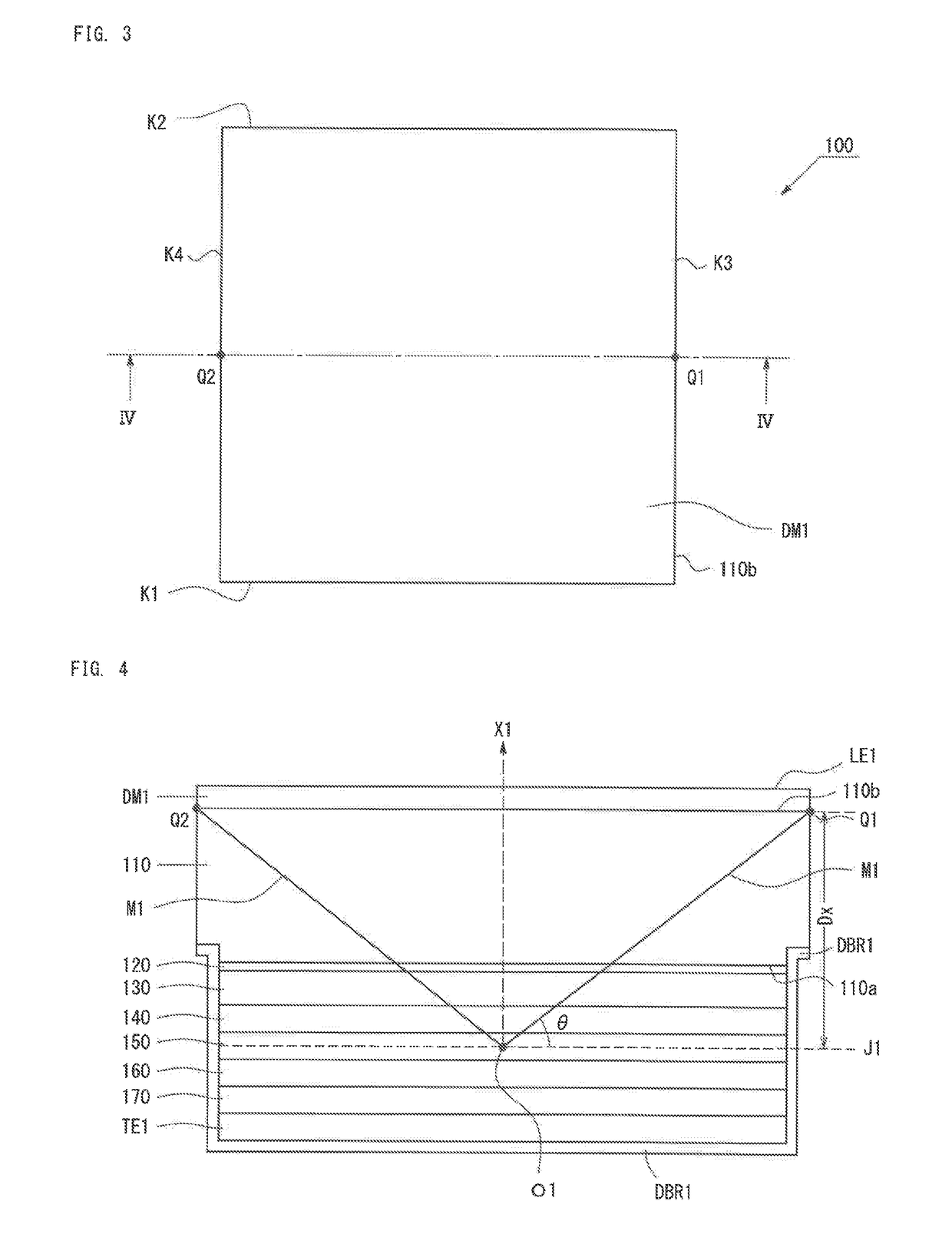
[0091]A light-emitting device was produced using a square substrate having a length of one side of 180 μm. Accordingly, the second surface is a square shape. A dielectric multilayer film was formed on the light extraction surface side of the light-emitting device. The dielectric multilayer film was formed by alternately depositing SiO2 and TiO2. A distributed bragg reflector was formed on the opposite side of the substrate when viewed from the light-emitting layer. The distributed bragg reflector was formed by alternately depositing SiO2 and TiO2. Four types of light-emitting devices having different thicknesses of the sapphire substrate were produced. In these four types of the light-emitting devices, a distance Dx between the surface of the substrate (corresponding to the second surface 110b) having the dielectric multilayer film thereon and the center surface of the light-emitting layer (corresponding to the center plane J1) is 40 μm, 60 μm, ...
PUM
 Abstract
Description
Claims
Application Information