Light-emitting device

Active Publication Date: 2011-07-05
EPISTAR CORP
View PDF4 Cites 8 Cited by
  • Summary
  • Abstract
  • Description
  • Claims
  • Application Information

AI Technical Summary

Benefits of technology

A wafer level chip scale package (WLCSP) is provided to achieve the purpose of a smaller size of LEDs package and a simpler package process, and increase the LEDs light extraction efficiency in the same time.

Problems solved by technology

Since the electronic products require light, thin, short, and small, how to reduce the LEDs package space and cost is a key issue.
Such LEDs package has difficulty to satisfy the light, thin, short, and small requirements because so many kinds of package materials stack together.

Method used


Image

  • Light-emitting device
  • Light-emitting device
  • Light-emitting device

Examples


first embodiment

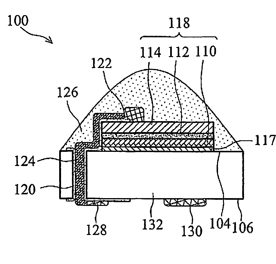
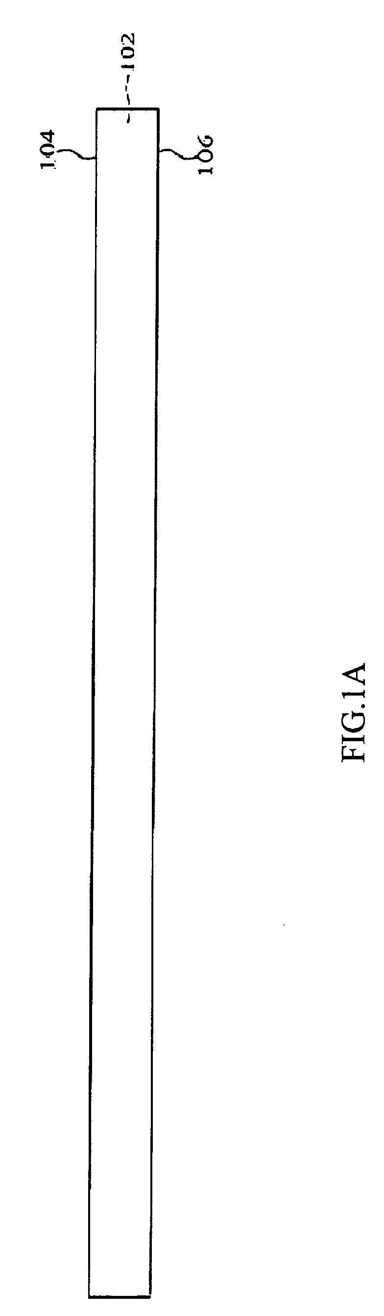
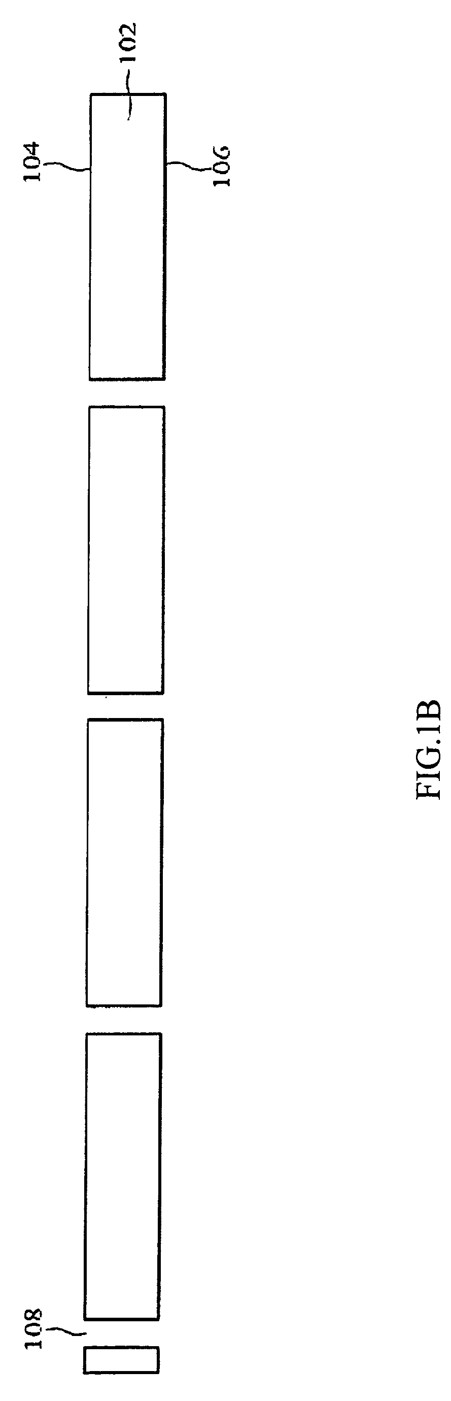
the present invention is illustrated in FIG. 1A to FIG. 1G. Referring to FIG. 1A, a wafer 102 including a first surface 104 and a second surface 106 is provided. The wafer is silicon wafer in this embodiment, and it is doped with the impurity of phosphorous or boron for increasing the conductivity. The wafer composition is not restricted in the present invention and can be other compositions or materials with good conductivity. Referring to FIG.1 B, a plurality of through-holes 108 are formed in the wafer 102 by laser. Referring to FIG.1C, a conductive adhesive layer 117 is formed to combine the semiconductor structure 116 with the wafer 102, then the sapphire substrate (not shown) is removed. The semiconductor structure 116 in this embodiment includes at least a buffer layer (not shown), a first conductive type semiconductor layer 114, an active layer 112, and a second conductive type semiconductor layer 110. In this embodiment, the first conductive type semiconductor layer 114 is ...


PUM


Abstract

The present invention is related to a light-emitting device. The present invention illustrates a vertical light-emitting device in one embodiment, comprising the following elements: a conductive substrate includes a through-hole, a patterned semiconductor structure disposed on a first surface of the substrate, a first bonding pad and a second bonding pad disposed on a second surface of the substrate, a conductive line passing through the through-hole connecting electrically the semiconductor structure layer, and an insulation layer on at least one sidewall of the through-hole insulates the conductive line form the substrate. The present invention illustrates a horizontal light-emitting device in another embodiment, comprising the following elements: a substrate includes a first tilted sidewall, a patterned semiconductor structure disposed on a first surface of the substrate, a first conductive line is disposed on at least the first tilted sidewall of the substrate and connecting electrically the patterned semiconductor structure.

Description

CROSS REFERENCE TO RELATED APPLICATIONSThis application claims the right of priority based on Taiwan Patent Application No. 097100674 entitled “Light-Emitting Device”, filed on Jan. 8, 2008, which is incorporated herein by reference and assigned to the assignee herein.TECHNICAL FIELDThe present invention generally relates to a light-emitting device, and more particularly to a light-emitting diode.BACKGROUNDLight-emitting diodes (LEDs) having advantages of low electricity consumption and high-speed power on-off response are versatile for different applications. Following the high-end cellular phone adopting LEDs as the back-lighting source, more and more electronic products intent to use LEDs. Since the electronic products require light, thin, short, and small, how to reduce the LEDs package space and cost is a key issue.LEDs with transparent substrate can be classified as a face up type and a flip chip type. The LEDs mentioned above may be mounted with the substrate side down onto a...

Claims


Application Information

Patent Timeline
IPC IPC(8): H01L33/00H01L33/20H01L33/32H01L33/38H01L33/48H01L33/62
CPCH01L33/385H01L24/24H01L24/82H01L33/20H01L33/32H01L33/486H01L33/62H01L2924/12041H01L2924/00
Inventor HSU, CHIA-LIANGLU, CHIH-CHIANGHUANG, CHIEN-FUWU, CHUN-YI
Owner EPISTAR CORP
Why Eureka
Try Eureka