

Semiconductor light emitting device
- Summary
- Abstract
- Description
- Claims
- Application Information
AI Technical Summary
Benefits of technology
Problems solved by technology
Method used
Image

Examples
example 1
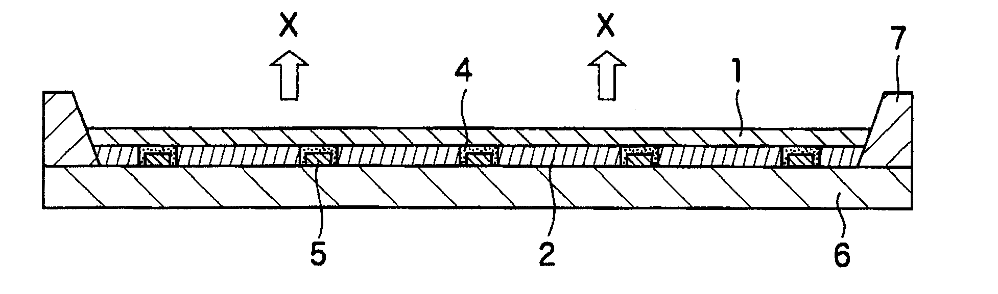
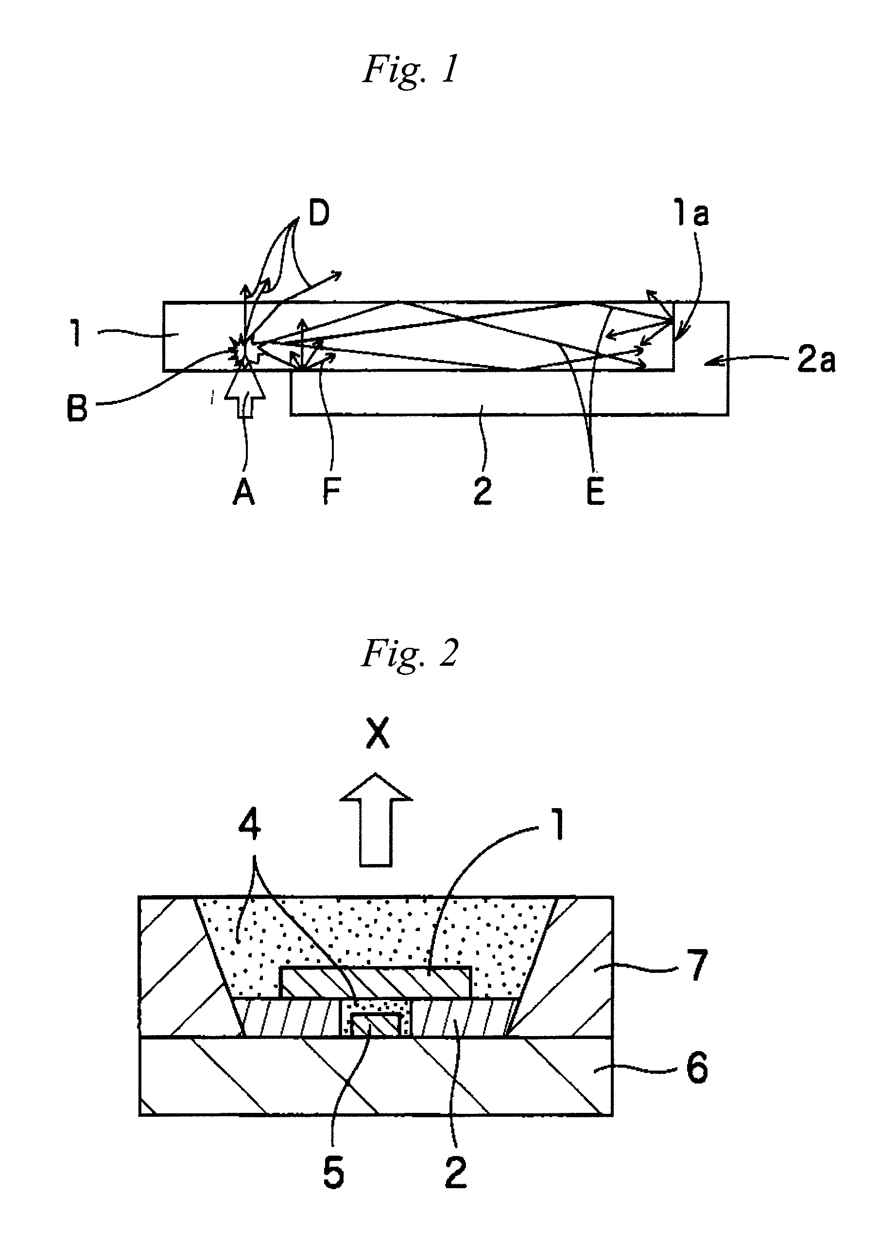
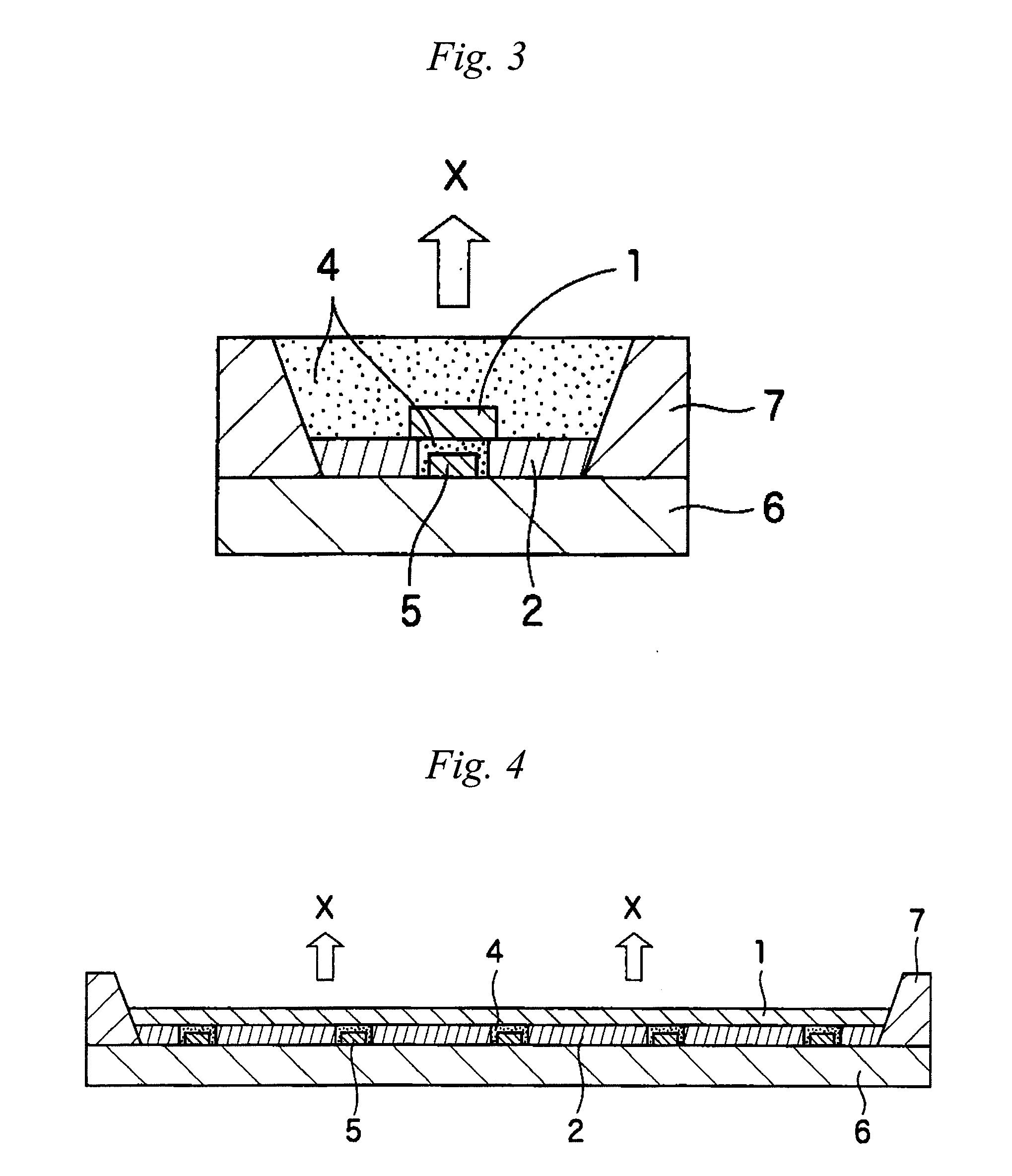
[0146]Using the LED element (four-blue-LEDs mounted type) shown in FIG. 13, an LED element for test was prepared. Namely, first, for the purpose of protecting respective four pieces of the LED chips including wire bonding with the gold wire, a minute amount of a thermosetting silicone elastomer (item No. KER 2500 manufactured by Shin-Etsu Silicone) was attached using a tip of a toothpick and temporarily cured at 100° C. for 15 min. Then, the resin composition for diffusive reflection resin layer formation prepared previously was formed over the whole inner surface (10 mm×10 mm) of the glass epoxy flame. On this occasion, care was taken so that the resin composition did not cover the LED chips. Thereafter, the resin composition was cured by heating at 100° C. for 1 hour and at 150° C. for 1 hour. Then, the silicone elastomer was added dropwise into the glass epoxy flame and a YAG plate diced into a size of 10 mm×10 mm was placed thereon with care so that no air bubbles remained, and ...
example 2
[0150]An LED element for test was prepared in accordance with Example 1 except that the LED element (sixteen-blue-LEDs mounted type) shown in FIG. 14 was used instead of the LED element (four-blue-LEDs mounted type) shown in FIG. 13. Namely, first, for the purpose of protecting respective sixteen pieces of the LED chips including wire bonding with the gold wire, a minute amount of a thermosetting silicone elastomer (item No. KER 2500 manufactured by Shin-Etsu Silicone) was attached using a tip of a toothpick and temporarily cured at 100° C. for 15 min. Then, the resin composition for diffusive reflection resin layer formation prepared previously was formed all over the whole inner surface (20 mm×20 mm) of the glass epoxy flame. On this occasion, care was taken so that the resin composition did not cover the LED chips. Thereafter, the resin composition was cured by heating at 100° C. for 1 hour and at 150° C. for 1 hour. Then, the silicone elastomer was added dropwise into the glass ...
example 3
[0154]An LED element for test was prepared in accordance with Example 2 except that the phosphor sheet (YAG sheet) having a size of 20 mm×20 mm was used instead of the phosphor plate (YAG plate).
PUM
 Abstract
Description
Claims
Application Information