Display device

a technology of a display device and a display screen, which is applied in the direction of semiconductor devices, basic electric elements, electrical appliances, etc., can solve the problems of reducing the lifespan and efficiency reducing the lifespan of the emitting layer, so as to reduce or minimize the damage of the light emitting layer

Active Publication Date: 2020-04-02
LG DISPLAY CO LTD
View PDF4 Cites 1 Cited by
  • Summary
  • Abstract
  • Description
  • Claims
  • Application Information

AI Technical Summary

Benefits of technology

[0006]The present disclosure provides a display device that can reduce or minimize damage of a light emitting layer.

Problems solved by technology

In the OLED device, there is a problem in that the light emitting layer is damaged through the photolithography process and a lifespan and efficiency thereof may decrease.

Method used


Image

  • Display device
  • Display device
  • Display device

Examples


first embodiment

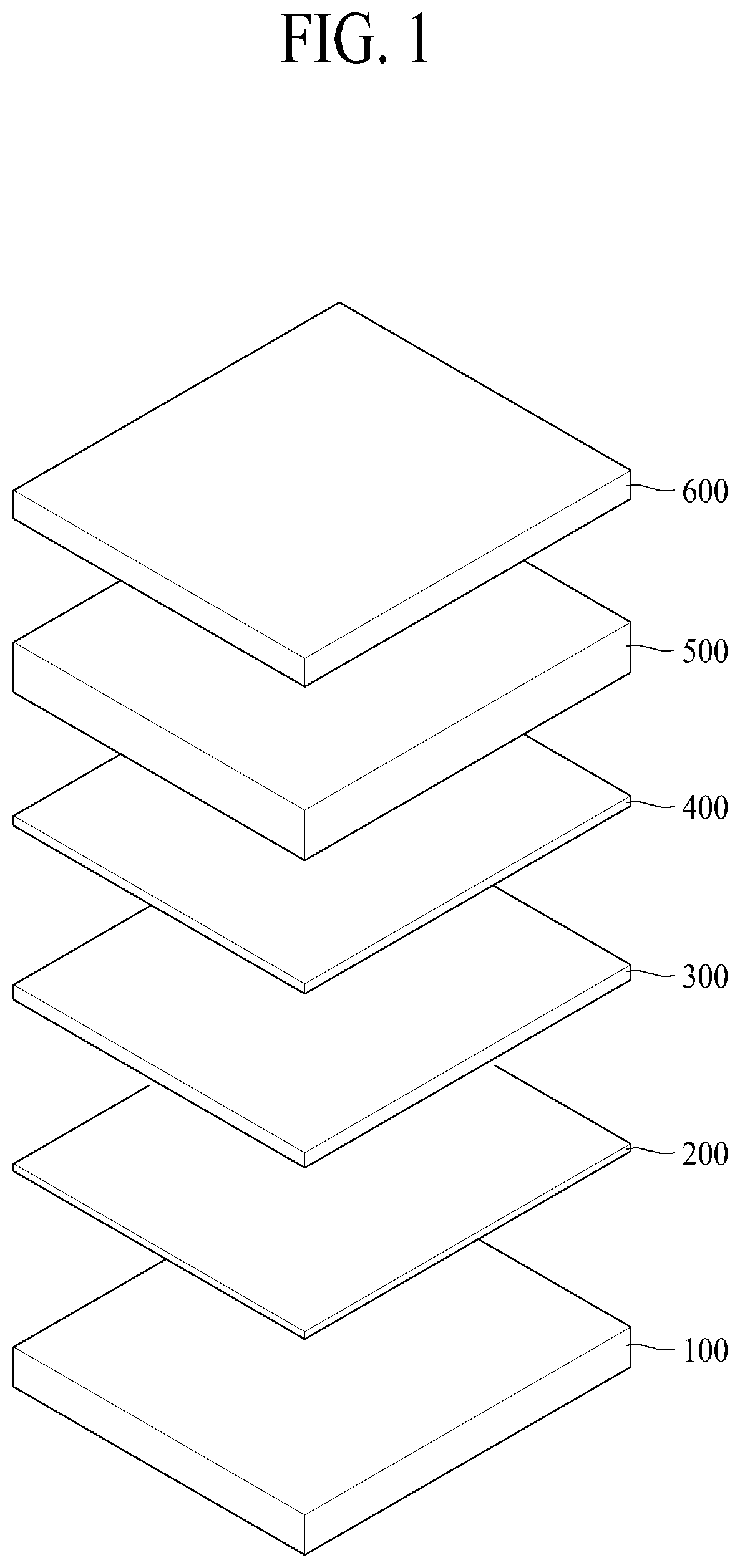
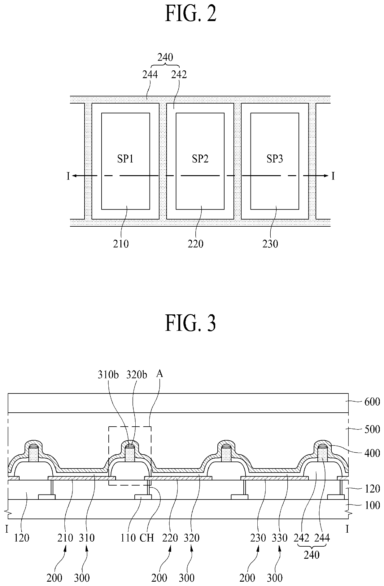
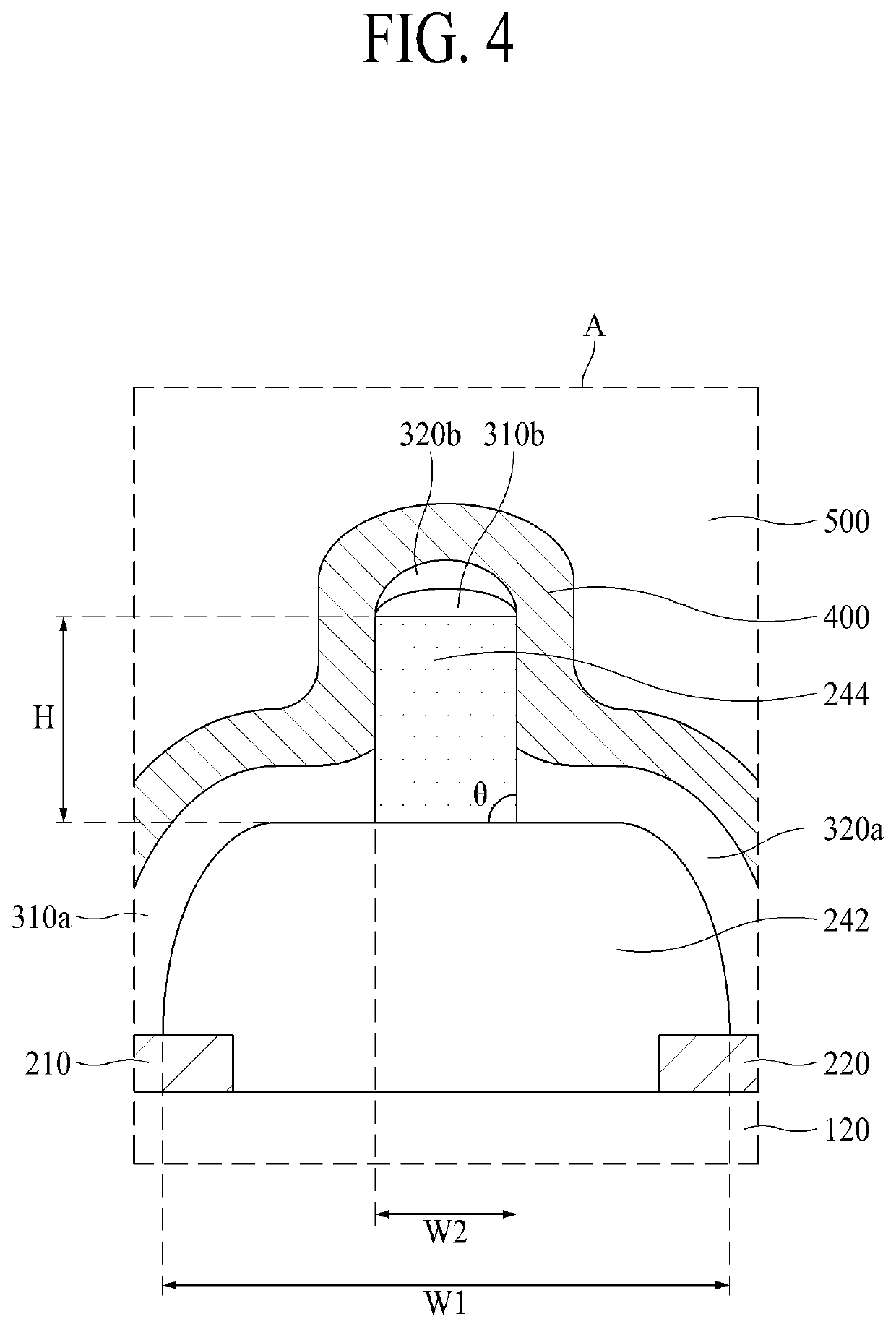
[0035]FIG. 1 is a perspective view schematically illustrating a display device according to an embodiment of the present disclosure. FIG. 2 is a plan view schematically illustrating subpixels according to a first embodiment of the present disclosure. FIG. 3 is a sectional view taken along line I-I in FIG. 2. FIG. 4 is an enlarged view illustrating an example of area A in FIG. 3. FIG. 5 is an enlarged view illustrating another example of area A in FIG. 3. FIG. 6 is an enlarged view illustrating still another example of area A in FIG. 3.

[0036]Referring to FIGS. 1, 2, and 3, a display device according to a first embodiment of the present disclosure includes a first substrate 100, a driving thin-film transistor 110, an insulating film 120, a first electrode200, a bank 240, a light emitting layer 300, a second electrode 400, an encapsulation film 500, and a second substrate 600.

[0037]The first substrate 100 is formed of glass or plastic, but the present disclosure is not limited thereto ...

second embodiment

[0091]FIG. 7 is a plan view schematically illustrating subpixels according to a second embodiment of the present disclosure. FIG. 8 is a sectional view taken along line II-II in FIG. 7. FIG. 9 is an enlarged view illustrating an example of area B in FIG. 8.

[0092]Referring to FIGS. 7, 8, and 9, a display device according to a second embodiment of the present disclosure includes a first substrate 100, a driving thin-film transistor 110, an insulating film 120, a first electrode 200, a bank 240, a light emitting layer 300, a second electrode 400, an encapsulation film 500, and a second substrate 600.

[0093]The first substrate 100, the driving thin-film transistor 110, the insulating film 120, the first electrode 200, the second electrode 400, the encapsulation film 500, and the second substrate 600 which are illustrated in FIGS. 7, 8, and 9 are substantially the same as the first substrate 100, the driving thin-film transistor 110, the insulating film 120, the first electrode 200, the s...


PUM

PropertyMeasurementUnit
angleaaaaaaaaaa
widthaaaaaaaaaa
heightaaaaaaaaaa

Abstract

A display device includes: a substrate having thereon a first subpixel, a second subpixel, and a third subpixel; a first electrode in each of the first to third subpixels on the substrate; a first bank between the first electrodes; a second bank on the first bank and having a width less than that of the first bank; a light emitting layer on the first electrodes, the first bank, and the second bank; and a second electrode on the light emitting layer. The light emitting layer provided on the second bank and the light emitting layer provided on the first bank are spaced apart from each other.

Description

CROSS-REFERENCE TO RELATED APPLICATIONS[0001]This application claims the benefit of and priority to Korean Patent Application No. 10-2018-0116080, filed on Sep. 28, 2018, which is hereby incorporated by reference in its entirety as if fully set forth herein.BACKGROUNDTechnical Field[0002]The present disclosure relates to a display device that displays an image.Description of the Related Art[0003]With advancement in information-oriented societies, demands for display devices that display an image have increased in various forms. Recently, various types of display devices such as a liquid crystal display (LCD) device, a plasma display panel (PDP) device, and an organic light emitting display (OLED) device have been widely utilized.[0004]An OLED device out of such display devices employs a spontaneous emission system, has a wide viewing angle, a high contrast ratio, and the like which are more excellent than those of an LCD device, and can be decreased in weight and thickness and is ad...

Claims


Application Information

Patent Timeline
Patent Type & Authority Applications(United States)
IPC IPC(8): H01L27/32H01L51/56
CPCH01L51/56H01L27/3246H01L2227/323H10K59/353H10K59/122H10K59/351H10K50/00H01L29/66833H10K71/00H10K59/1201
Inventor YANG, YUCHEOLKIM, SUHYEON
Owner LG DISPLAY CO LTD
Why Eureka
Try Eureka