Selector devices for a memory cell

a technology of selector devices and memory cells, applied in the direction of basic electric elements, semiconductor devices, electrical equipment, etc., can solve the problems of high production cost, prior art selector devices can consume too much power, and selector devices that cannot scale with reram devices to achieve the required current density of tens

Pending Publication Date: 2020-05-21
THE RES FOUND OF STATE UNIV OF NEW YORK
View PDF2 Cites 6 Cited by
  • Summary
  • Abstract
  • Description
  • Claims
  • Application Information

AI Technical Summary

Benefits of technology

[0010]The present disclosure offers advantages and alternatives over the prior art by providing a selector device that has a first electrode and a second electrode with a selector layer disposed therebetween. The first electrode is composed of a first metal having a first work function. The second electrode is composed of a second metal that has a second work function. The selector layer has a conduction band and a valence

Problems solved by technology

Problematically however, prior art selector devices do not scale with ReRAM devices to achieve the required current densities of tens of mega amps per centimeter squared (MA/cm2), i.e. diodes.
Additionally, some selector devices, such as phase-change selector devices, may contain high contents of arsen

Method used


Image

  • Selector devices for a memory cell
  • Selector devices for a memory cell
  • Selector devices for a memory cell

Examples


Embodiment Construction

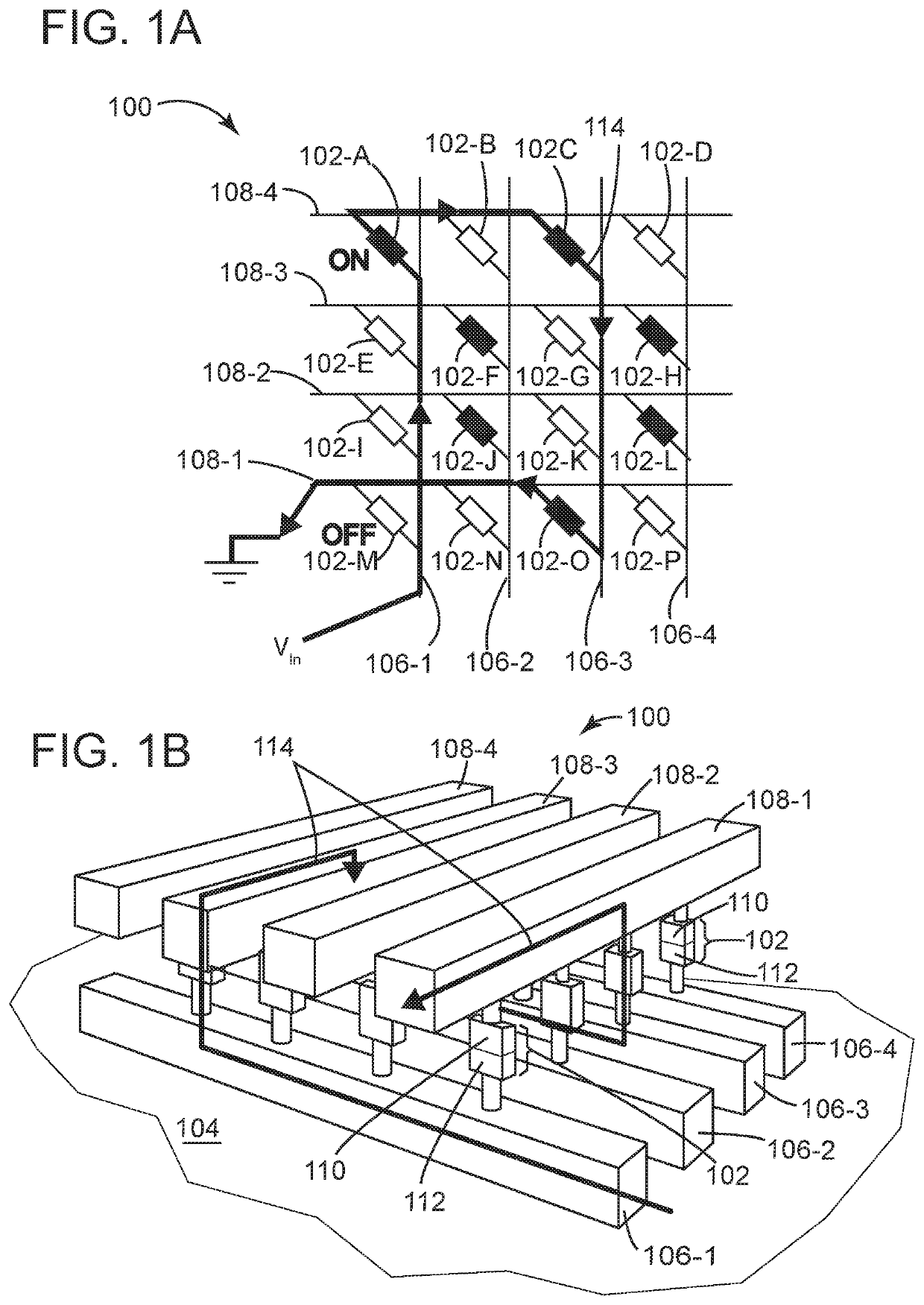
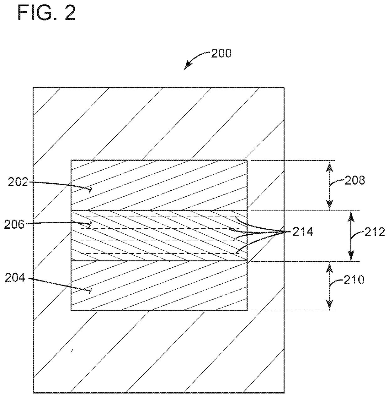
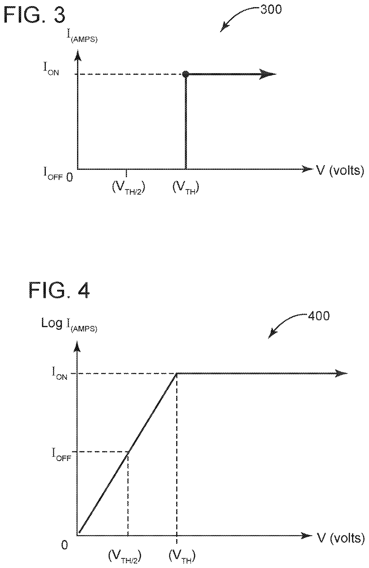
[0027]Certain examples will now be described to provide an overall understanding of the principles of the structure, function, manufacture, and use of the methods, systems, and devices disclosed herein. One or more examples are illustrated in the accompanying drawings. Those skilled in the art will understand that the methods, systems, and devices specifically described herein and illustrated in the accompanying drawings are non-limiting examples and that the scope of the present disclosure is defined solely by the claims. The features illustrated or described in connection with one example may be combined with the features of other examples. Such modifications and variations are intended to be included within the scope of the present disclosure.

[0028]The terms “substantially”, “approximately”, “about”, “relatively,” or other such similar terms that may be used throughout this disclosure, including the claims, are used to describe and account for small fluctuations, such as due to v...


PUM


Abstract

A selector device includes a first electrode composed of a first metal having a first work function. A second electrode is composed of a second metal having a second work function. A selector layer is disposed between the first and second electrodes and is composed of a dielectric material having a conduction band and a valence band defining a band gap of at least 5 electron volts. Dopant atoms are disposed in the selector layer to form a sub-conduction band that is below the conduction band and above the work functions. When a threshold voltage is applied across the first and second electrodes, and a magnitude of the threshold voltage exceeds an energy difference between the sub-conduction band and the work functions, but does not exceed an energy difference between the conduction band and the work functions, an on-current will conduct through the selector layer.

Description

GOVERNMENT RIGHTS STATEMENT[0001]This invention was made with U.S. Government support under Agreement Nos. FA8750-11-1-0008 and FA8750-16-1-0063 awarded by the Air Force Research Labs to the SUNY Research Foundation for the State University of New York. The Government has certain rights in the invention.TECHNICAL FIELD[0002]The present disclosure relates to selector devices for a memory cell and methods of making the same. More specifically, the disclosure relates to metal-insulator-metal selector devices for two terminal resistive switching memory cells and methods of making the same.BACKGROUND[0003]Two terminal resistive switching memory devices (herein resistive memory devices), such as resistive random access memory (ReRAM) devices, phase change memory (PCM) devices, conductive bridge random access memory (CBRAM) devices or the like, show great promise as enablers of neuromorphic computer systems. Much like a synapse in a human brain, several types of resistive memory devices ca...

Claims


Application Information

Patent Timeline
IPC IPC(8): H01L27/24H01L45/00
CPCH01L45/1253H01L45/146H01L27/2418H01L45/1641H10B63/22H10B63/80H10N70/00H10N70/24H10N70/8833H10N70/063H10N70/826H10N70/041H10N70/841
Inventor BECKMANN, KARSTENCADY, NATHANIEL
Owner THE RES FOUND OF STATE UNIV OF NEW YORK
Why Eureka
Try Eureka