Method of forming a device structure using selective deposition of gallium nitride and system for same

Active Publication Date: 2020-06-18
ASM IP HLDG BV
View PDF3 Cites 183 Cited by
  • Summary
  • Abstract
  • Description
  • Claims
  • Application Information

AI Technical Summary

Problems solved by technology

Although gallium nitride has many desirable properties, gallium nitride substrates are relatively expensive, compared to silicon substrates.
While such processes wo

Method used


Image

  • Method of forming a device structure using selective deposition of gallium nitride and system for same
  • Method of forming a device structure using selective deposition of gallium nitride and system for same
  • Method of forming a device structure using selective deposition of gallium nitride and system for same

Examples


Embodiment Construction

[0018]The description of exemplary embodiments provided below is merely exemplary and is intended for purposes of illustration only; the following description is not intended to limit the scope of the disclosure or the claims. Moreover, recitation of multiple embodiments having stated features is not intended to exclude other embodiments having additional features or other embodiments incorporating different combinations of the stated features. Further, the illustrations presented herein are not meant to be actual views of any particular material, structure, or device, but are merely idealized representations that are used to describe embodiments of the disclosure.

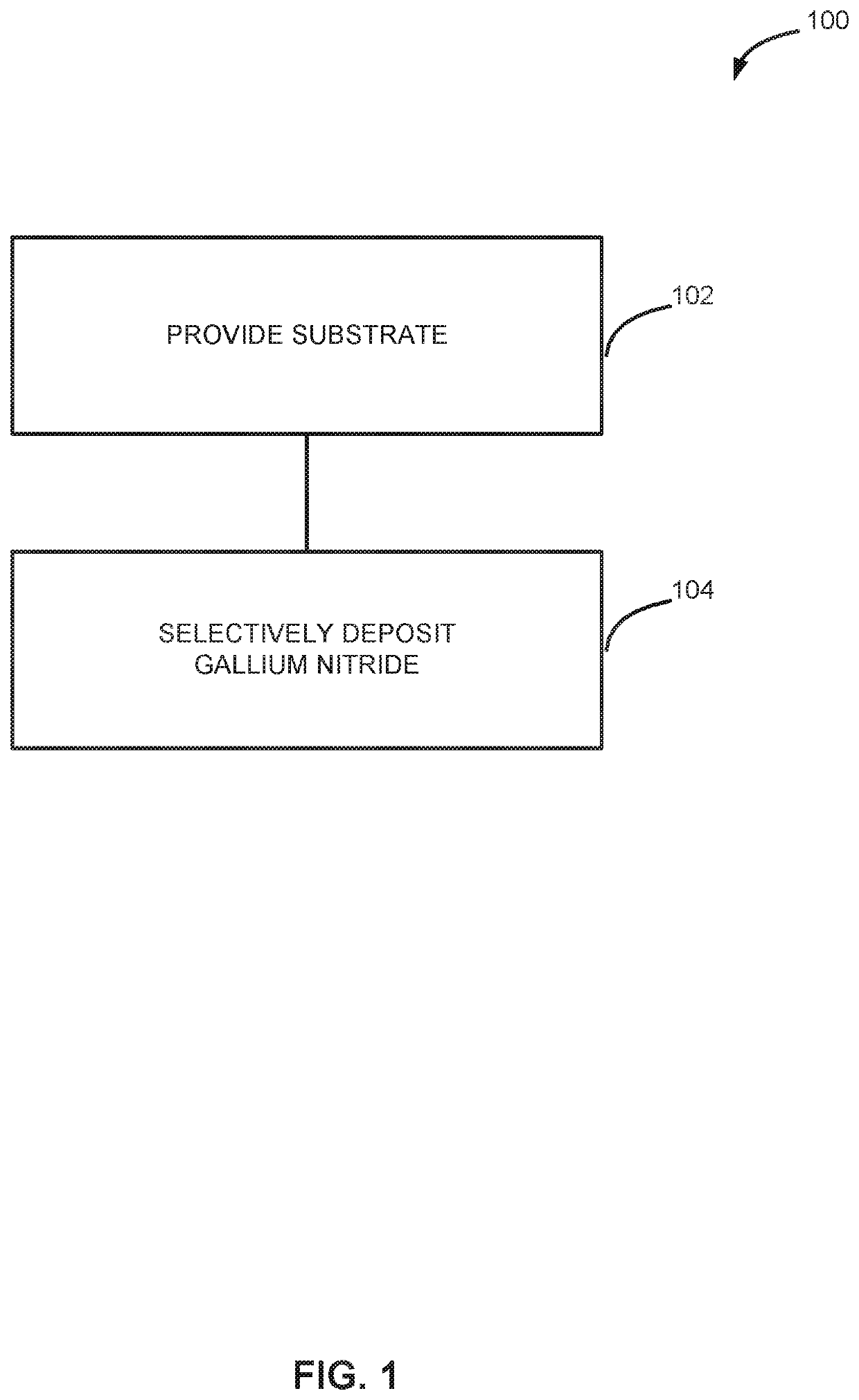
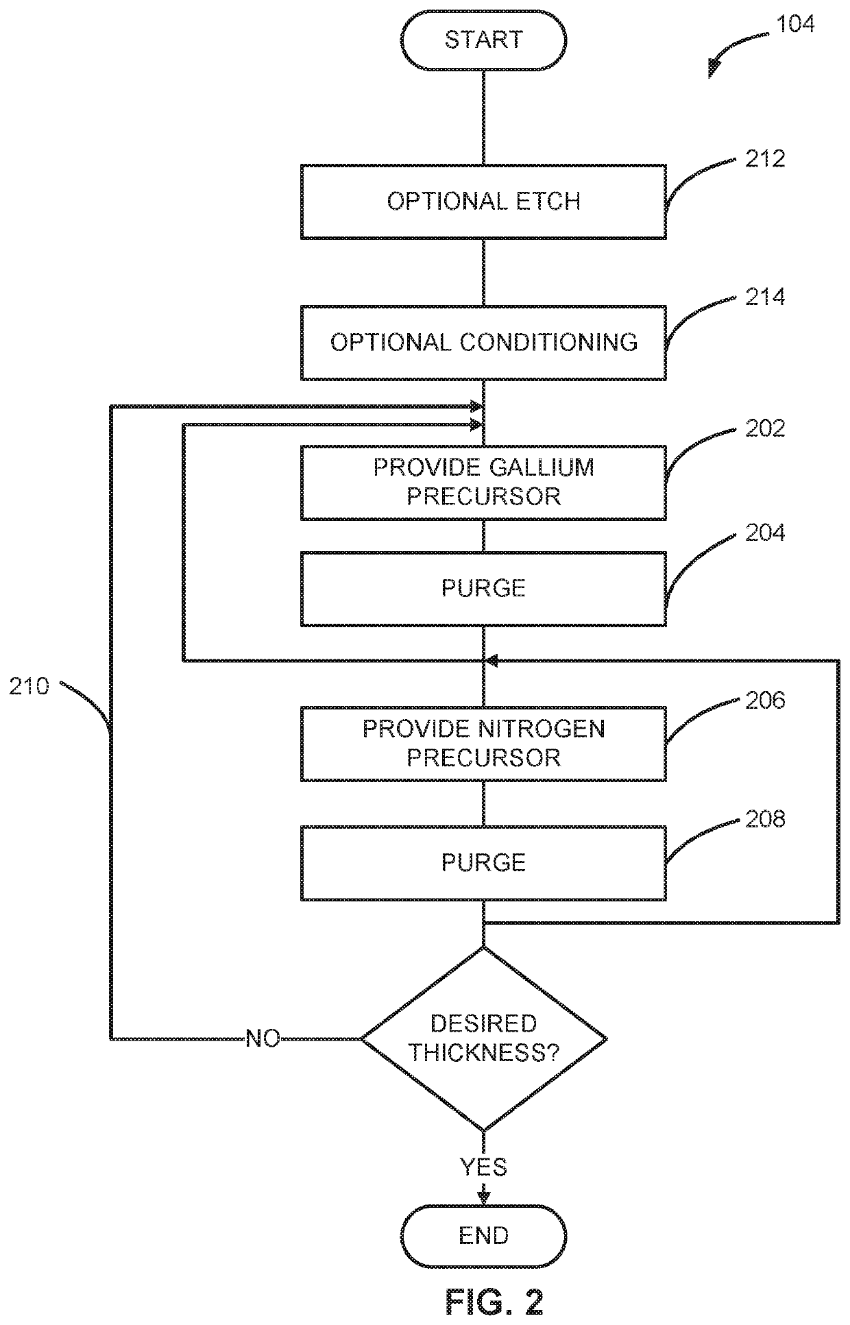
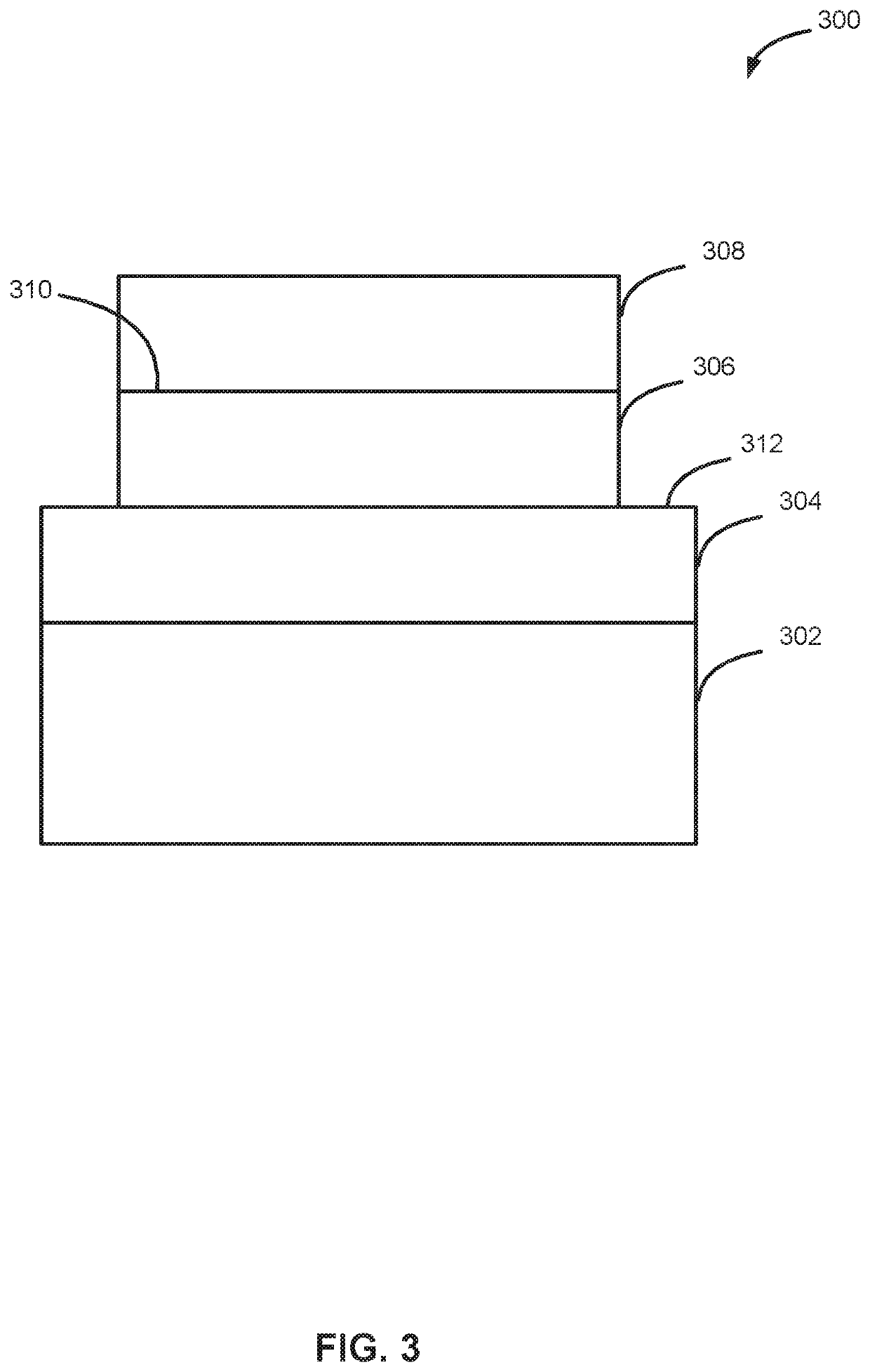
[0019]The present disclosure generally relates to methods of forming structures and to structures formed using the methods. The methods and structures described herein can be used to form a variety of devices, such as, for example, devices that include monocrystalline and / or polycrystalline gallium nitride layers.

[0020]As ...


PUM

PropertyMeasurementUnit
Temperatureaaaaaaaaaa
Fractionaaaaaaaaaa

Abstract

A method of forming a device structure including a selectively-deposited gallium nitride layer is disclosed.

Description

CROSS-REFERENCE TO RELATED APPLICATIONS[0001]This application is a nonprovisional application of, and claims priority to and the benefit of, U.S. Provisional Patent Application Ser. No. 62 / 779,684, filed Dec. 14, 2018 and entitled METHOD OF FORMING A DEVICE STRUCTURE USING SELECTIVE DEPOSITION OF GALLIUM NITRIDE AND SYSTEM FOR SAME, which is hereby incorporated by reference.FIELD OF THE DISCLOSURE[0002]The present disclosure generally relates to thin-film deposition methods, to structures formed using the methods, and to systems for performing the methods. More particularly, the disclosure relates to methods of selectively depositing gallium nitride to form device structures and to related structures and systems.BACKGROUND OF THE DISCLOSURE[0003]Gallium nitride (GaN) is a direct bandgap material that exhibits relatively high electron mobility and a relatively wide bandgap, compared to silicon. Accordingly, gallium nitride has gained increasing attention for use in a variety of devic...

Claims


Application Information

Patent Timeline
IPC IPC(8): H01L21/02H01L21/306C23C16/56C23C16/30C23C16/455
CPCH01L21/30612C23C16/303H01L21/0254H01L21/02636C23C16/45527C23C16/56H01L21/0262H01L21/02458H01L21/02617H01L21/67207H01L21/02502C23C16/0272C23C16/04C23C16/45534C30B29/406C30B25/16C23C16/34C23C16/045C23C16/45553H01L21/02389
Inventor BANERJEE, SOURISHAARNINK, ANTONIUSKOVALGIN, ALEXEY
Owner ASM IP HLDG BV
Why Eureka
Try Eureka