Semiconductor package

Inactive Publication Date: 2020-10-01
POWERCHIP SEMICON MFG CORP
View PDF0 Cites 0 Cited by
  • Summary
  • Abstract
  • Description
  • Claims
  • Application Information

AI Technical Summary

Benefits of technology

[0005]The invention provides a semiconductor package that can have hig

Problems solved by technology

However, as the demand for the drivers to have small size and/or high operation speeds is increased, the TCP has been gradually replaced by the COF due to its circuit pitch and bonding pitch being inferior to the COF.
Recently, as the users demand higher d

Method used


Image

  • Semiconductor package
  • Semiconductor package

Examples


Example

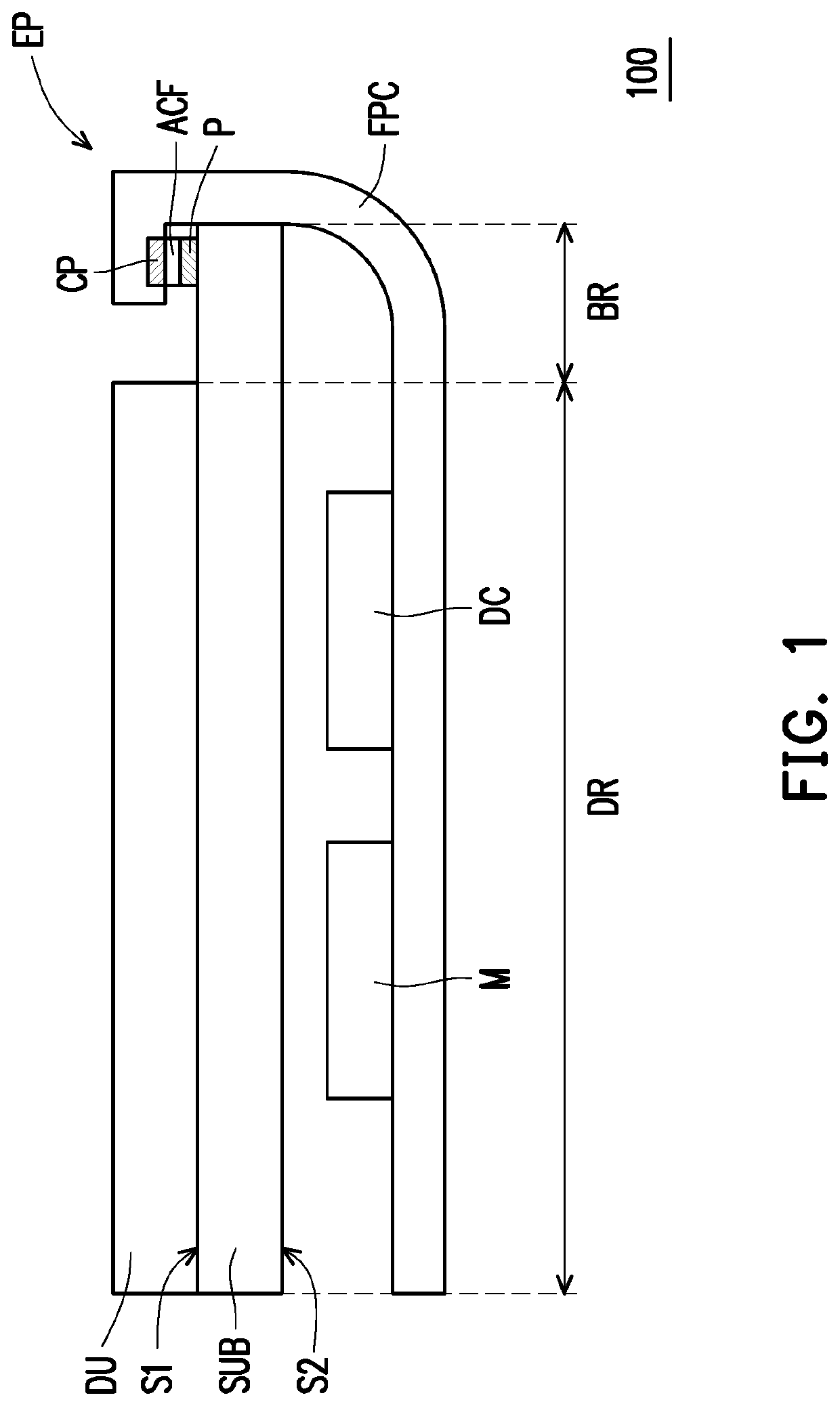
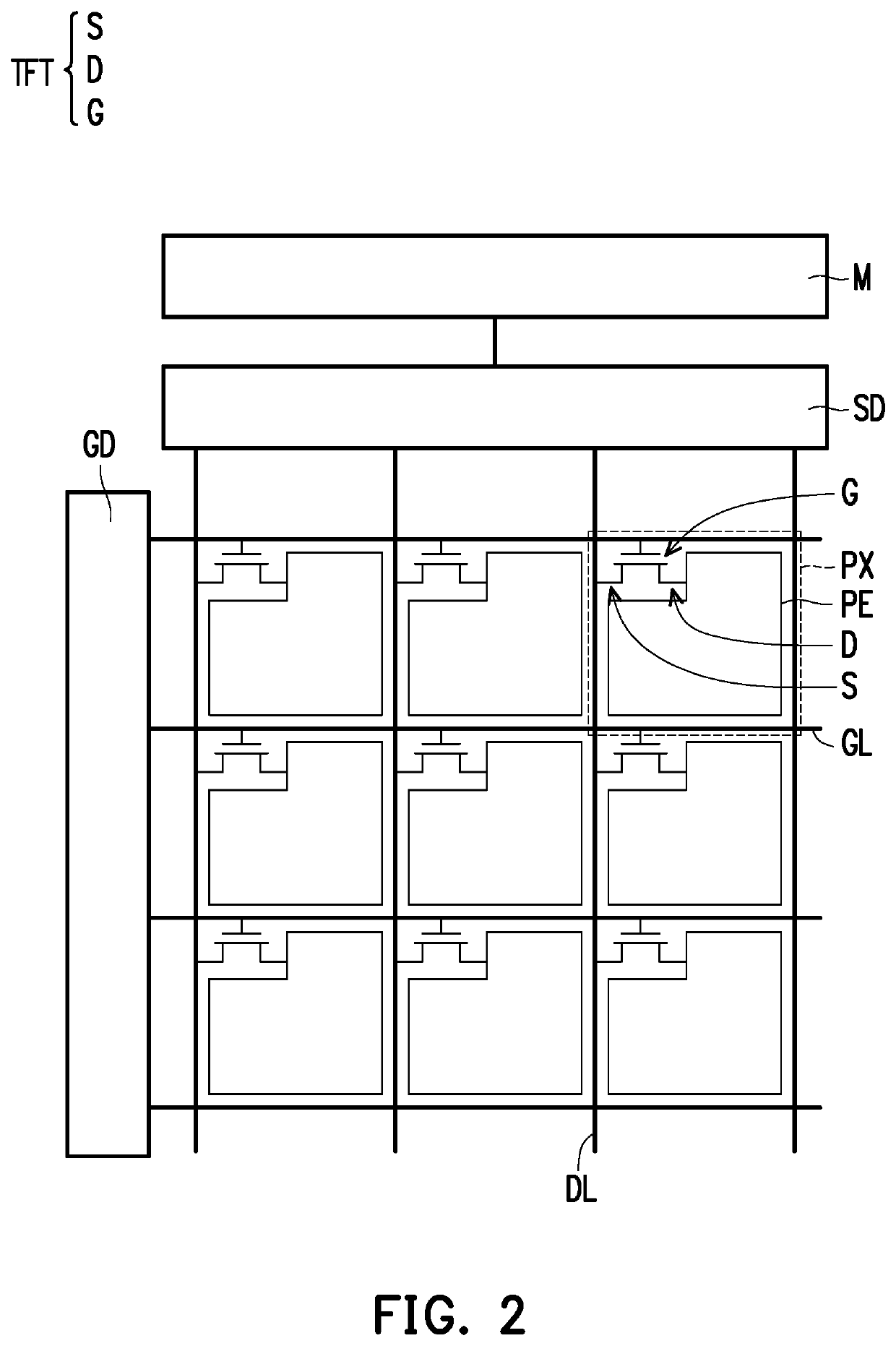
[0022]In the following detailed description, for purposes of explanation, numerous specific details are set forth in order to provide a thorough understanding of the disclosed embodiments. It will be apparent, however, that one or more embodiments may be practiced without these specific details. In other instances, well-known structures and devices are schematically shown in order to simplify the drawing.

[0023]The invention will be described more comprehensively below with reference to the drawings for the embodiments. However, the invention may also be implemented in different forms rather than being limited by the embodiments described in the invention. Thicknesses of layer and region in the drawings are enlarged for clarity. The same reference numbers are used in the drawings and the description to indicate the same or like parts, which are not repeated in the following embodiments.

[0024]It will be understood that when an element is referred to as being “on” or “connected” to ano...


PUM


Abstract

The present disclosure provides a semiconductor package including a substrate, a display unit, a flexible circuit board, a driving circuit, and a memory. The substrate has a first surface and a second surface opposite to each other, and the first surface has a display region and a bonding region. The display unit is disposed on the display region of the first surface. The flexible circuit board is disposed below the second surface and has a connection portion extended to the bonding region of the first surface. The driving circuit is disposed on the flexible circuit board and electrically connects to the display unit. The memory is disposed on the flexible circuit board and electrically connects to the driving circuit.

Description

CROSS-REFERENCE TO RELATED APPLICATION[0001]This application claims the priority benefit of Taiwan application serial no. 108110759, filed on Mar. 27, 2019. The entirety of the above-mentioned patent application is hereby incorporated by reference herein and made a part of this specification.BACKGROUND OF THE INVENTION1. Field of the Invention[0002]The invention relates to a package structure, and more particularly, to a semiconductor package. cl 2. Description of Related Art[0003]With the development of display technology, the demand for a driver with high-integration IC that capable of driving a display unit after connection (also referred to as a driver IC) is increased, and thus various semiconductor packages have been developed. In general, a common semiconductor package for driving the display unit may be, for example, a chip on glass (COG), a tape carrier package (TCP), or a chip on film (COF). The TCP and COF can make the display to have a narrow border design compared to th...

Claims


Application Information

Patent Timeline
IPC IPC(8): H05K1/18H01L27/32H01L23/00H01L23/538G02F1/1345G09G3/20
CPCG09G3/2092H01L27/3276H01L2924/14511H01L23/5387H05K1/189H05K2201/10128H05K2201/10136G02F1/13452H01L2924/1438H05K2201/056H01L2224/32227H01L2924/1426H05K1/118H05K2201/10159H01L2924/1437H01L24/32H01L25/18G02F1/1345G09G3/3648H01L2924/15156H01L2924/15192H05K3/361H05K3/323H10K50/841H01L23/50H01L23/13H01L23/4985H01L24/06H10K59/131
Inventor CHEN, CHUN-LIANGHSU, HANN-JYE
Owner POWERCHIP SEMICON MFG CORP
Why Eureka
Try Eureka