Solid-state imaging element, imaging device, and control method of solid-state imaging element
a control method and imaging element technology, applied in the direction of color television, television system, radio control device, etc., can solve problems such as difficulty in dealing with a case, and achieve the effect of excellent effect of reducing the scale of the circui
- Summary
- Abstract
- Description
- Claims
- Application Information
AI Technical Summary
Benefits of technology
Problems solved by technology
Method used
Image

Examples
first embodiment
1. First Embodiment
[0078][Configuration Example of Imaging Device]
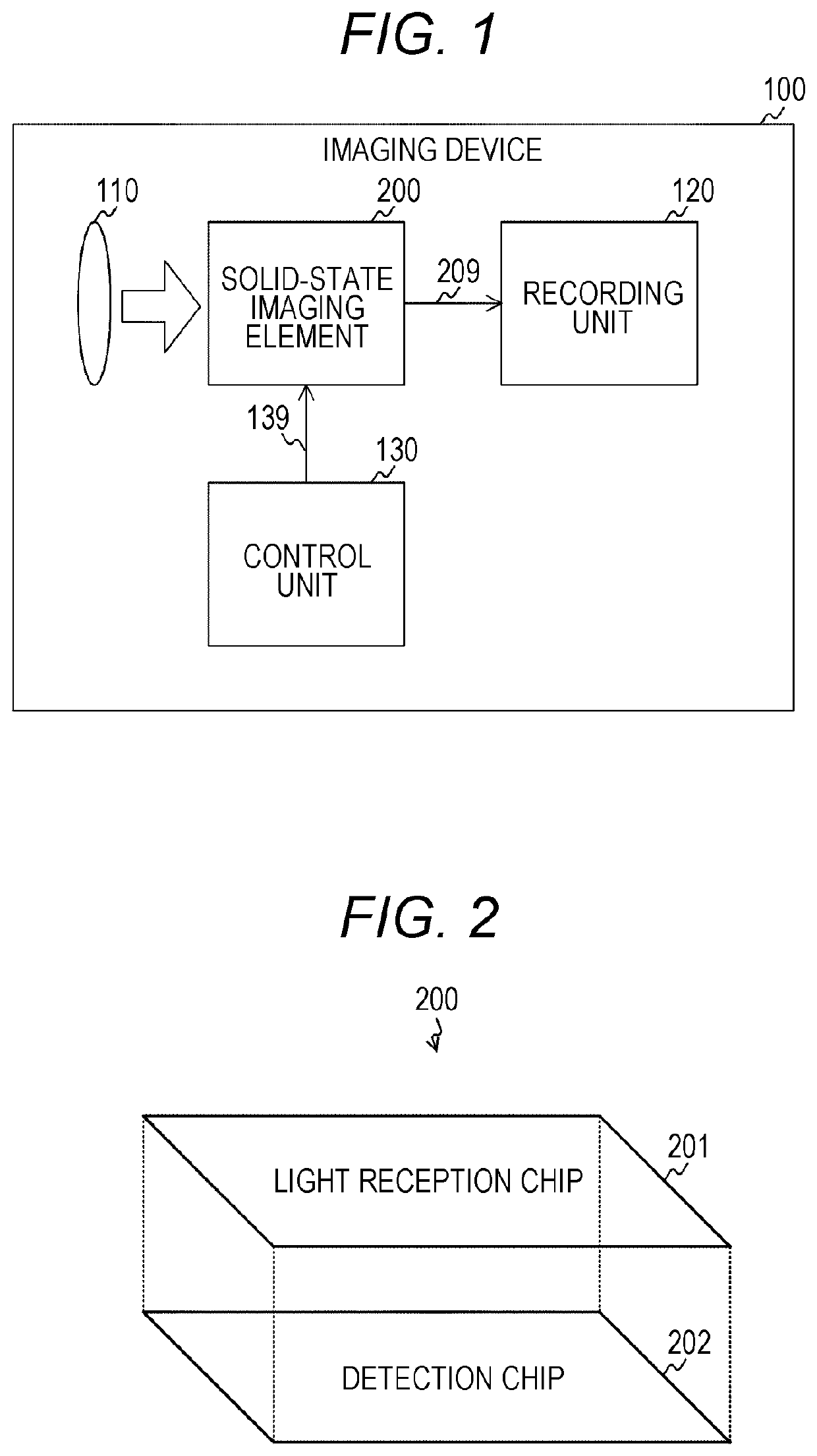
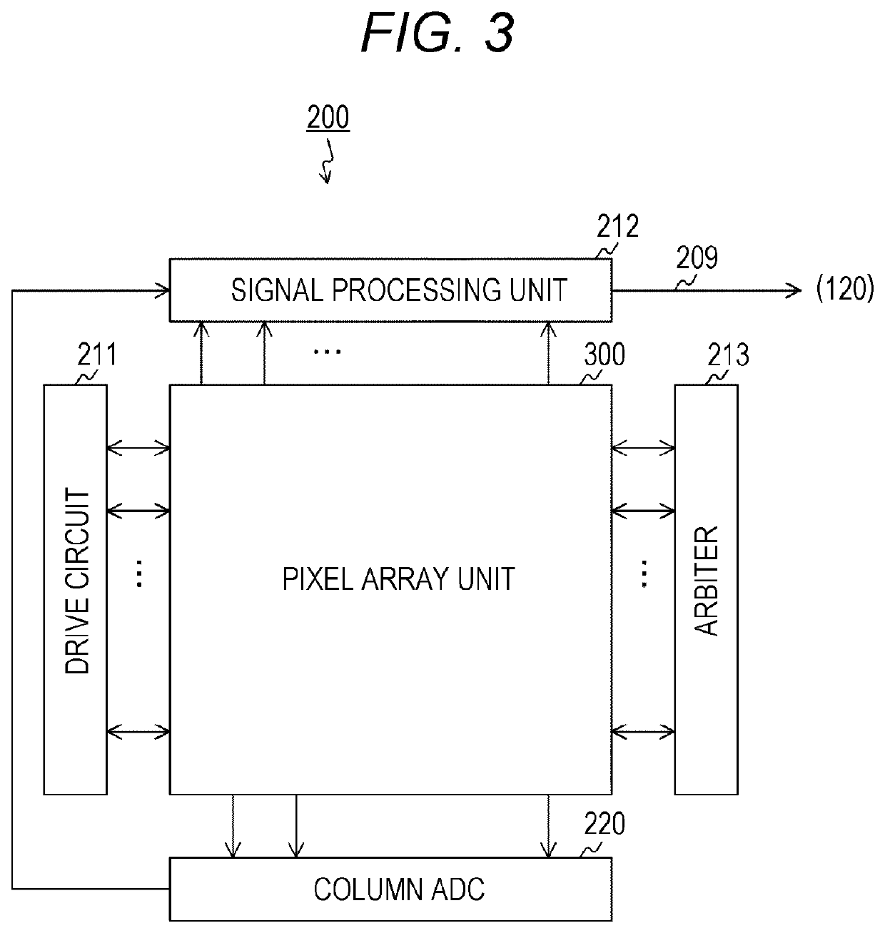
[0079]FIG. 1 is a block diagram illustrating a configuration example of an imaging device 100 in a first embodiment of the present technology. The imaging device 100 is provided with an imaging lens 110, a solid-state imaging element 200, a recording unit 120, and a control unit 130. As the imaging device 100, a camera mounted on an industrial robot, an in-vehicle camera and the like are assumed.
[0080]The imaging lens 110 condenses incident light and guides the same to the solid-state imaging element 200. The solid-state imaging element 200 photoelectrically converts the incident light to image image data. The solid-state imaging element 200 executes predetermined signal processing such as image recognition processing on the imaged image data, and outputs data indicating a processing result and a detection signal of an address event to the recording unit 120 via a signal line 209. A generating method of the detection ...
second embodiment
2. Second Embodiment
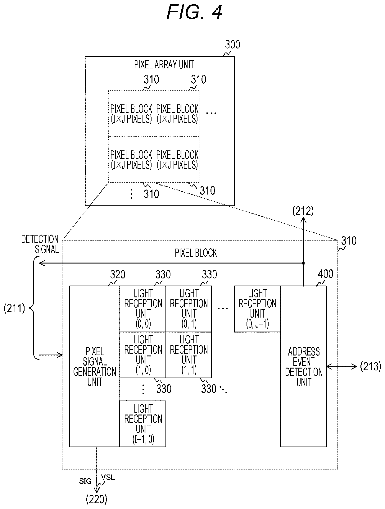
[0159]Although the pixel signal generation unit 320 is provided for each pixel block 310 in the above-described first embodiment, there is a possibility that the circuit scale of the solid-state imaging element 200 increases as the number of pixels increases. A solid-state imaging element 200 in a second embodiment is different from that in the first embodiment in that pixel signal generation units 320 are reduced.
[0160]FIG. 15 is a block diagram illustrating a configuration example of a pixel array unit 300 in the second embodiment of the present technology. The pixel array unit 300 is different from that in the first embodiment in that the pixel signal generation unit 320 is not provided.
[0161]Furthermore, an address event detection unit 400 in the second embodiment is different from that in the first embodiment in generating a pixel signal SIG and outputting the same via a vertical signal line VSL.
[0162]FIG. 16 is a circuit diagram illustrating a configuration...
third embodiment
3. Third Embodiment
[0186]In the above-described second embodiment, the capacitors 431 and 433 are arranged in the address event detection unit 400; however, the gain is deteriorated when the capacitance C1 is reduced according to expression 5, so that it is difficult to improve an operation speed of the circuit by reducing the capacitance C1. A solid-state imaging element 200 according to a third embodiment is different from that in the second embodiment in that a capacitor 431 is arranged for each pixel to improve an operation speed.
[0187]FIG. 22 is a block diagram illustrating a configuration example of a pixel array unit 300 in the third embodiment of the present technology. The pixel array unit 300 in the third embodiment is different from that in the second embodiment in that each of light reception units 330 generates a pixel signal SIG in place of an address event detection unit 400. Furthermore, a vertical signal line VSL is wired for each column of pixels, for example. Then...
PUM
| Property | Measurement | Unit |
|---|---|---|
| threshold | aaaaa | aaaaa |
| electric signal | aaaaa | aaaaa |
| voltage | aaaaa | aaaaa |
Abstract
Description
Claims
Application Information
 - R&D Engineer
- R&D Manager
- IP Professional
- Industry Leading Data Capabilities
- Powerful AI technology
- Patent DNA Extraction
Browse by: Latest US Patents, China's latest patents, Technical Efficacy Thesaurus, Application Domain, Technology Topic.
© 2024 PatSnap. All rights reserved.Legal|Privacy policy|Modern Slavery Act Transparency Statement|Sitemap