Image processing device and method of electronic device

a technology of image processing and electronic devices, which is applied in the field of image processing devices and electronic devices, can solve the problems of face image, mounting space, and pattern of structured light, and achieve the effects of saving mounting space, improving the quality of infrared image, and saving mounting spa

Active Publication Date: 2021-02-04
SAMSUNG ELECTRONICS CO LTD
View PDF0 Cites 2 Cited by
  • Summary
  • Abstract
  • Description
  • Claims
  • Application Information

AI Technical Summary

Benefits of technology

[0011]To obtain an infrared image of a good quality, an electronic device of various embodiments may remove a pattern included in the infrared image which has been obtained using a structured light, without using an additional auxiliary light source (e.g., an IR LED, illuminator). An electronic device of various embodiments may save a mounting space, a price and power consumption of the auxiliary light source, and improve a quality of the restored infrared image by using a deformed pattern being based on depth information as a mask.

Problems solved by technology

For example, when the infrared camera acquires a face image by using the structured light, the face image may be overlaid with the pattern of the structured light and thus may be heavily distorted.
When the auxiliary light source is added besides the structured light in order to acquire the good-quality infrared image, the electronic device may cause problems such as a mounting space, a price, power consumption, etc.

Method used


Image

  • Image processing device and method of electronic device
  • Image processing device and method of electronic device
  • Image processing device and method of electronic device

Examples


Embodiment Construction

[0019]Various embodiments of the present disclosure are described below in detail with reference to the accompanying drawings.

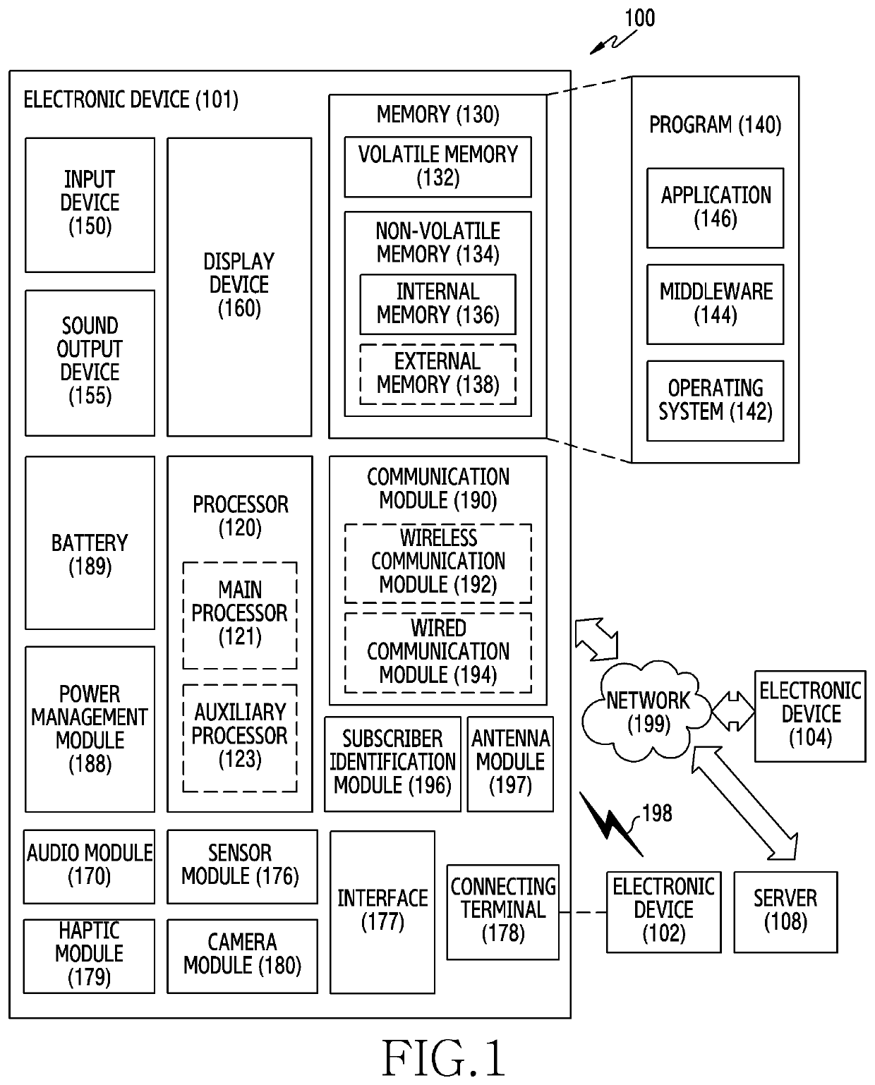
[0020]FIG. 1 is a block diagram illustrating an electronic device 101 in a network environment 100 according to various embodiments.

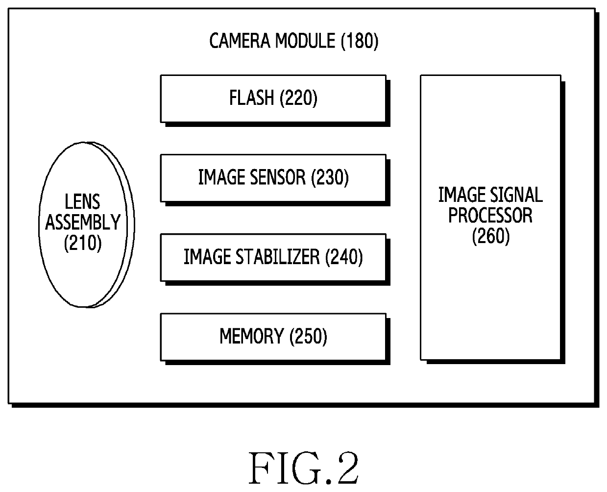
[0021]Referring to FIG. 1, the electronic device 101 in the network environment 100 may communicate with an electronic device 102 via a first network 198 (e.g., a short-range wireless communication network), or an electronic device 104 or a server 108 via a second network 199 (e.g., a long-range wireless communication network). According to an embodiment, the electronic device 101 may communicate with the electronic device 104 via the server 108. According to an embodiment, the electronic device 101 may include a processor 120, memory 130, an input device 150, a sound output device 155, a display device 160, an audio module 170, a sensor module 176, an interface 177, a haptic module 179, a camera module 180, a power management mo...


PUM


Abstract

According to various embodiments of the present invention, an electronic device can comprise: a light source configured to allow light, excluding a visible light band, to be incident on a designated pattern; a memory for storing designated pattern information; a camera configured to receive the light, which is incident from the light source and reflected by an external object; and a processor. The processor can be configured to: acquire a first image on an external object by using a camera, wherein the first image includes a pattern formed when the designated pattern is deformed by a curve of the surface of the external object; extract deformed pattern information from the first image by using the first image and the designated pattern information; and generate a second image from which the pattern deformed in the first image has been removed, by using the first image and the extracted deformed pattern information. Additional various embodiments are possible.

Description

CROSS-REFERENCE TO RELATED APPLICATIONS[0001]This application is a 371 of International Application No. PCT / KR2019 / 002409 filed on Feb. 28, 2019, which claims priority to Korean Patent Application No. 10-2018-0026170 filed on Mar. 6, 2018, the disclosures of which are herein incorporated by reference in their entirety.1. FIELD[0002]The present disclosure relates to a device and method capable of providing an infrared image from which a pattern of a structured light has been removed, in an electronic device.2. DESCRIPTION OF RELATED ART[0003]As the performance of an electronic device is improved, various services and additional functions presented through the electronic device are being increased gradually. Also, to increase an effective value of the electronic device and satisfy various desires of users, various applications executable in the electronic device are being developed.[0004]Among these applications, there are even those related with a camera function. By using a camera m...

Claims


Application Information

Patent Timeline
Patent Type & Authority Applications(United States)
IPC IPC(8): G06T5/00G06T7/521H04N5/33G06V10/141G06V10/143G06V10/98
CPCG06T5/001G06T2207/10048H04N5/33G06T7/521H04N9/31G06V40/166G06V10/98G06V10/141G06V10/143G06V10/273H04N23/00G06T7/557H04N9/315G06V10/94G06T2207/30168H04N23/51
Inventor KEH, YONGCHANPARK, BYEONGHOONYOON, YOUNGKWON
Owner SAMSUNG ELECTRONICS CO LTD
Why Eureka
Try Eureka