Pixel circuit for top-emitting amoled panel and driving method thereof

Active Publication Date: 2021-03-18
SHENZHEN CHINA STAR OPTOELECTRONICS SEMICON DISPLAY TECH CO LTD
View PDF0 Cites 0 Cited by
  • Summary
  • Abstract
  • Description
  • Claims
  • Application Information

AI Technical Summary

Benefits of technology

The present invention provides a pixel circuit and driving method for a top-emitting AMOLED panel that can effectively address the problem of IR voltage drop caused by impedance increase of the transparent cathode and prevent circuit failure caused by VSS voltage rise while keeping the voltage difference between VDD and VSS without increasing power consumption. This invention is particularly suitable for large-size top-emitting AMOLED panels.

Problems solved by technology

As the resolution increases, the aperture area of the bottom-emitting AMOLED is greatly restricted.
The transparent cathode of the current large-size top-emitting AMOLED panel has a high impedance, resulting in serious IR drop.

Method used


Image

  • Pixel circuit for top-emitting amoled panel and driving method thereof
  • Pixel circuit for top-emitting amoled panel and driving method thereof
  • Pixel circuit for top-emitting amoled panel and driving method thereof

Examples


Embodiment Construction

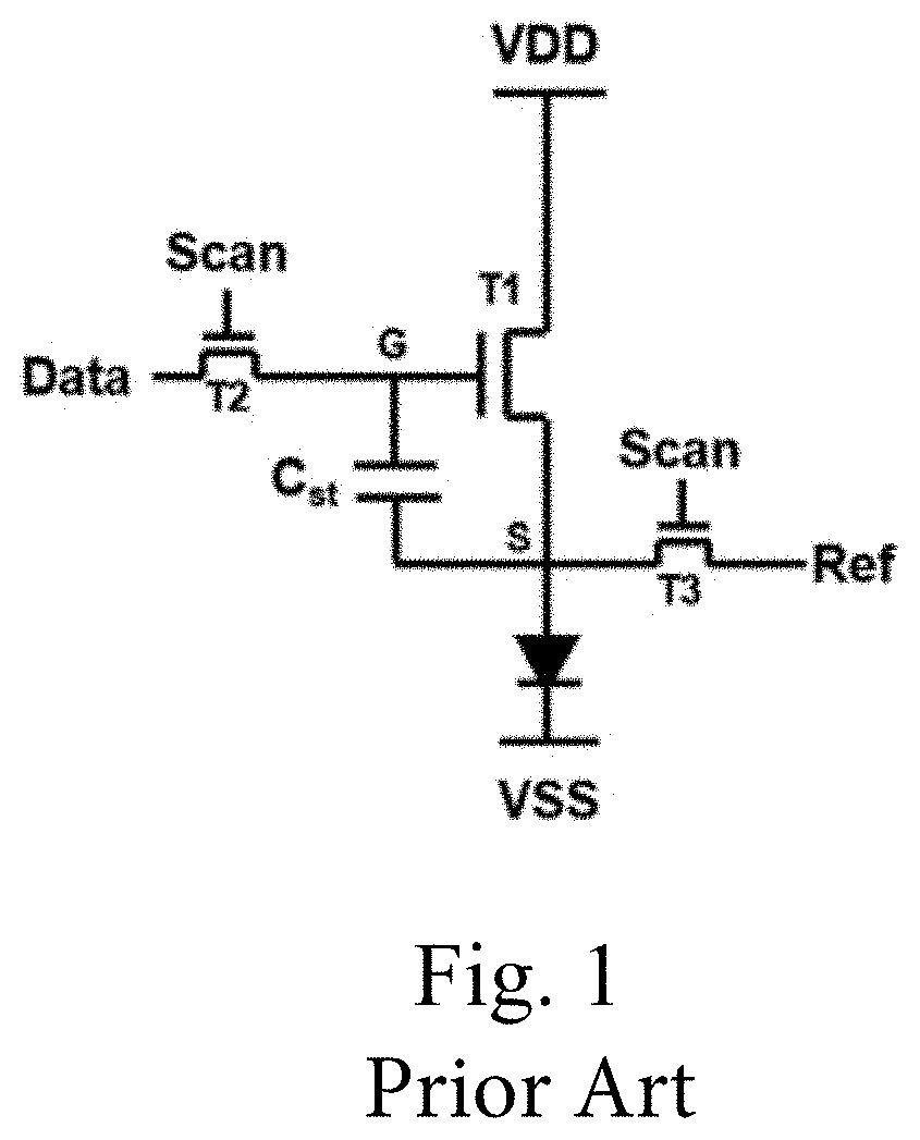
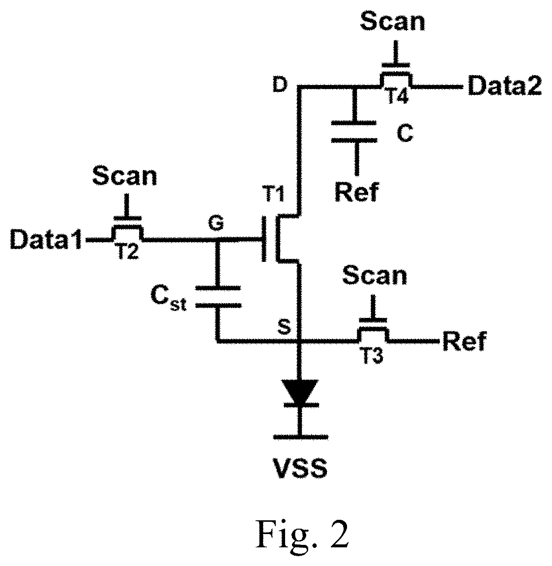
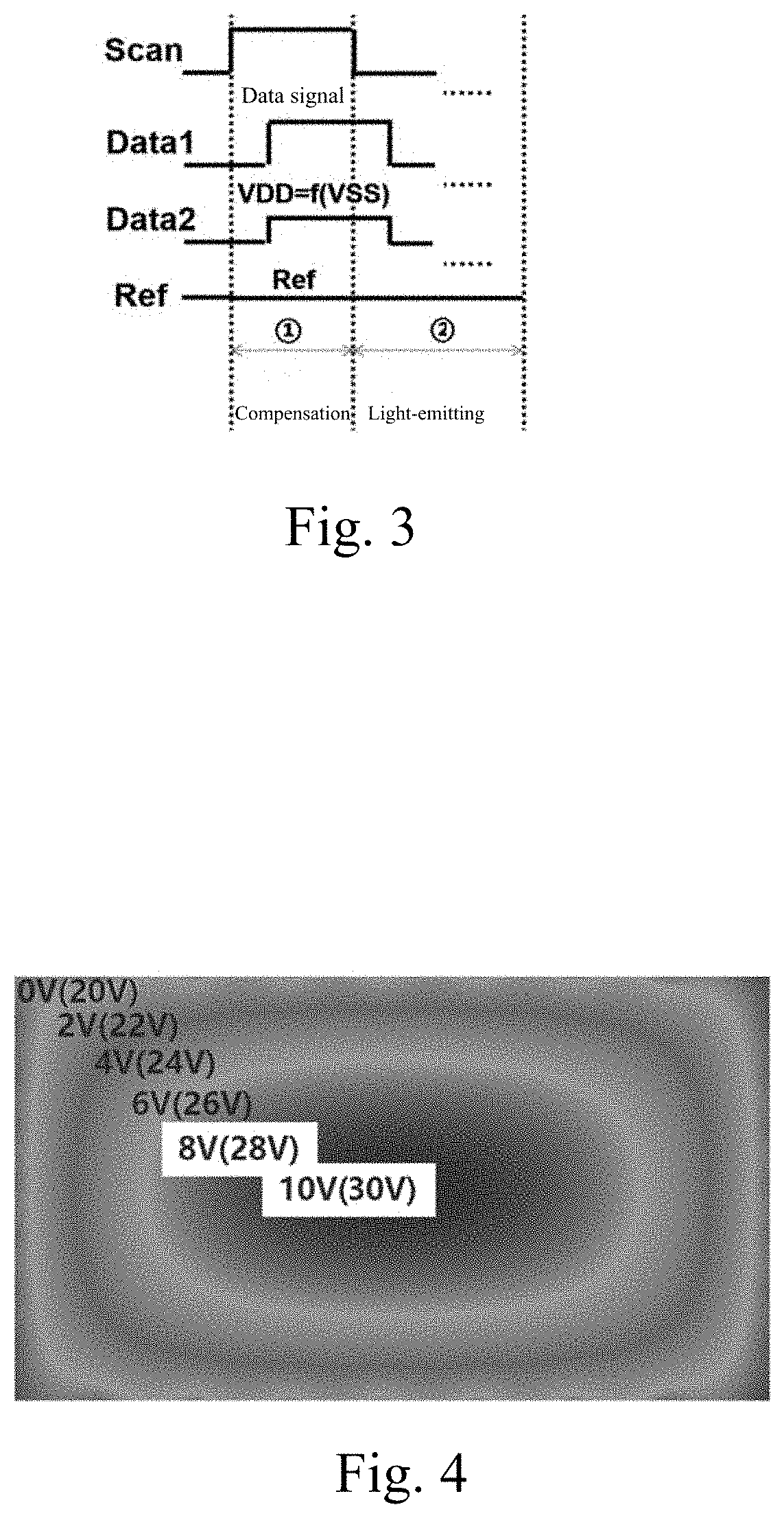
"d_n">[0047]Referring to FIG. 2 and FIG. 3, FIG. 2 is a schematic view showing the structure of a preferred embodiment of a pixel circuit for each of multiple pixels that are arranged in a matrix form in top-emitting AMOLED panel of the present invention; FIG. 3 is a schematic view showing the signal timing sequence of the preferred embodiment of the pixel circuit of the top-emitting AMOLED panel of the present invention. The preferred embodiment is a 4T2C pixel circuit, comprising: four TFTs T1-T4, and two capacitor Cst and C; wherein T1 serving as a driving TFT, T1, having a gate connected to node G, a source and a drain connected respectively to node S and node D; T2, having a gate connected to scan signal Scan, a source and a drain connected respectively to node G and data signal Data1; T3, having a gate connected to scan signal Scan, a source and a drain connected respectively to node S and reference voltage Ref; T4, having a gate connected to scan signal Scan, a source and a d...


PUM


Abstract

A top-emitting AMOLED panel includes a pixel circuit for each of multiple pixels. The circuit includes a first TFT connected to first, second, and third nodes; a second TFT connected to a scan signal, the first node and a data signal; a third TFT connected to the scan signal, the second node, and a reference voltage; a fourth TFT connected to the scan signal, the third node, and a high voltage power source; a first capacitor connected to the first node and the second node; a second capacitor connected to the third node and the reference voltage; and an OLED connected to the second node and a low voltage power source. The voltages supplied from the high voltage power source and the low voltage power source to the pixel are variable as functions of the location of the pixel on the panel, such that a voltage difference therebetween keeps unchanged.

Description

CROSS REFERENCE TO RELATED APPLICATIONS[0001]This is a continuation-in-part application of co-pending U.S. patent application Ser. No. 15 / 579,948, filed on Dec. 6, 2017, which is a national stage of PCT Application No. PCT / CN2017 / 111007, filed on Nov. 15, 2017, claiming foreign priority of Chinese Patent Application No. 201710736699.1, filed on Aug. 24, 2017, the disclosure of which is incorporated herein by reference in its entirety.BACKGROUND OF THE INVENTION1. Field of the Invention[0002]The present invention relates to the field of display techniques, and in particular to a pixel circuit for top-emitting AMOLED panel and driving method thereof.2. The Related Arts[0003]The organic light-emitting diode (OLED) has the advantages of low power consumption, wide color gamut, high brightness, high resolution, wide viewing angle, and fast response time, and attracts much attention.[0004]The driving types of OLED can be divided, according to the driving method, into the passive matrix OL...

Claims


Application Information

Patent Timeline
IPC IPC(8): G09G3/3258G09G3/3266
CPCG09G3/3258G09G3/3266G09G3/3233G09G2300/0426G09G2300/0814G09G2300/0876G09G2300/0861
Inventor HAN, BAIXIANG
Owner SHENZHEN CHINA STAR OPTOELECTRONICS SEMICON DISPLAY TECH CO LTD
Why Eureka
Try Eureka