

Full adder cell with improved power efficiency
a full adder and power efficiency technology, applied in the field of adder circuits, can solve the problems of occupying significant chip space, requiring thousands of transistors for full adders, and proving difficult to improve on legacy mirror-style cmos full adder cells
- Summary
- Abstract
- Description
- Claims
- Application Information
AI Technical Summary
Benefits of technology
Problems solved by technology
Method used
Image

Examples
Embodiment Construction
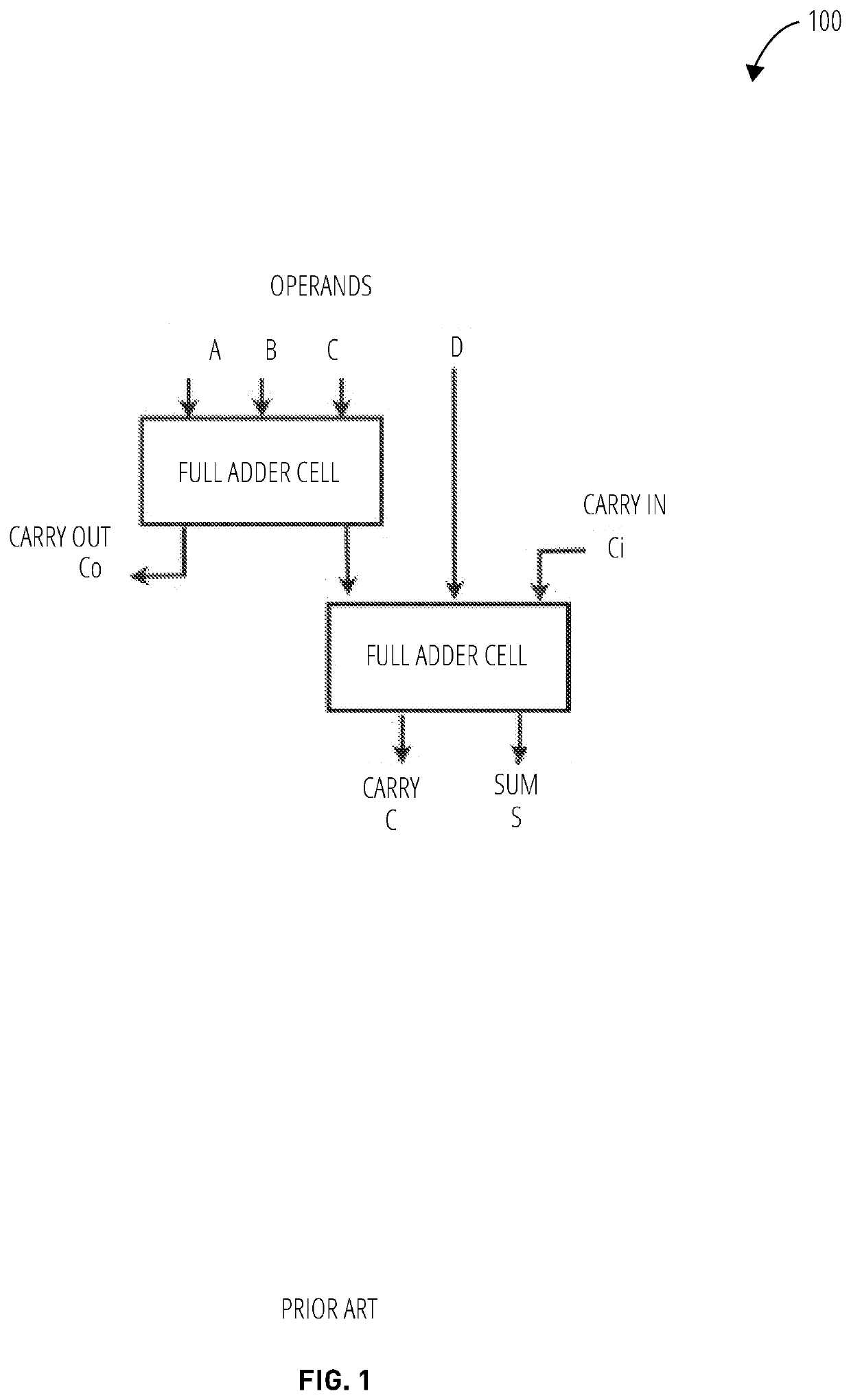
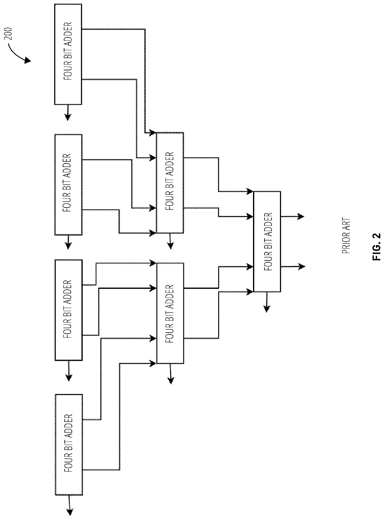
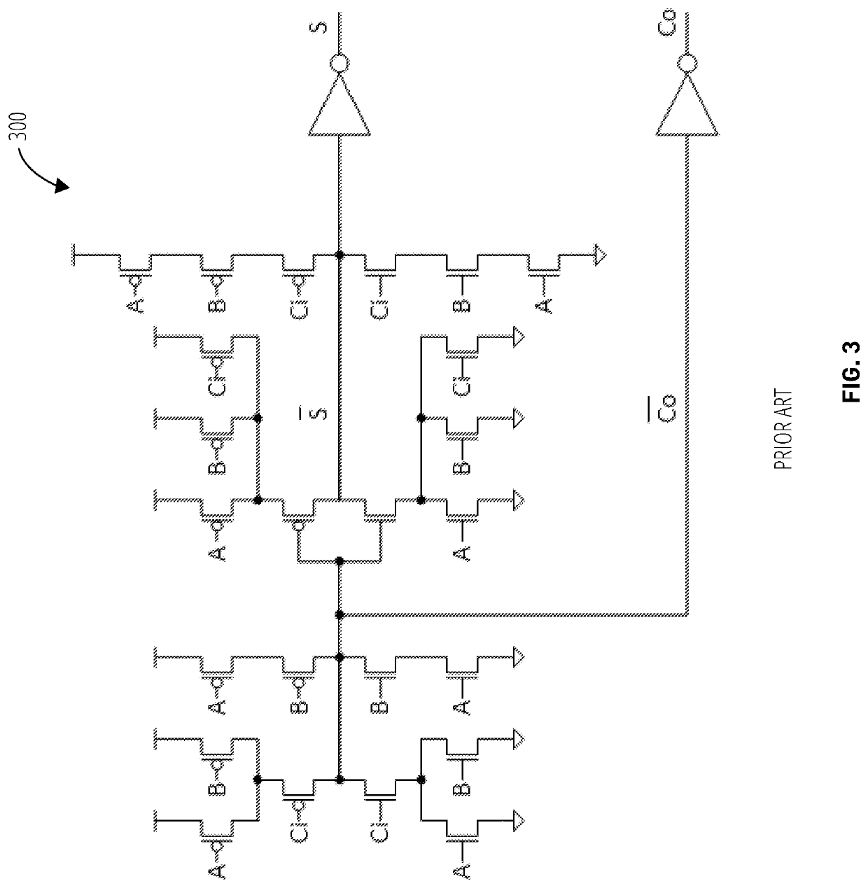
lass="d_n">[0024]Embodiments of a full adder circuit (also referred to as a full adder cell) are disclosed utilizing a first-stage two-input exclusive NOR gate of A and B inputs implemented as a two-input NAND gate (NAND2) combined with an OR-AND-INVERTER (OAI21) cell. The disclosed full adder circuit demonstrates improved power characteristics over conventional full adder circuits while maintaining or improving performance, for example when utilized to form 4:2 compressors, 5:2 compressors, or higher-order compressors.
[0025]This disclosure uses various terms that should be accorded the following meaning unless otherwise indicated. “Control terminal” refers to the terminal of a circuit at which a control input is applied. “Control input” refers to a signal applied to a circuit to control the operation of the circuit on transforming or passing one or more signals at its input terminals to its output terminals. “Input terminal” refers to the terminal of a circuit at which an input sig...
PUM
 Abstract
Description
Claims
Application Information