
High speed, universal polarity full adder which consumes minimal power and minimal area

a full adder, universal polarity technology, applied in the field of full adders, can solve the problems of increasing the total power dissipation and the total cell area, and the high device count and the high device stacking

Inactive Publication Date: 2007-02-27
NAT SEMICON CORP
View PDF7 Cites 15 Cited by
  • Summary
  • Abstract
  • Description
  • Claims
  • Application Information

AI Technical Summary

Benefits of technology

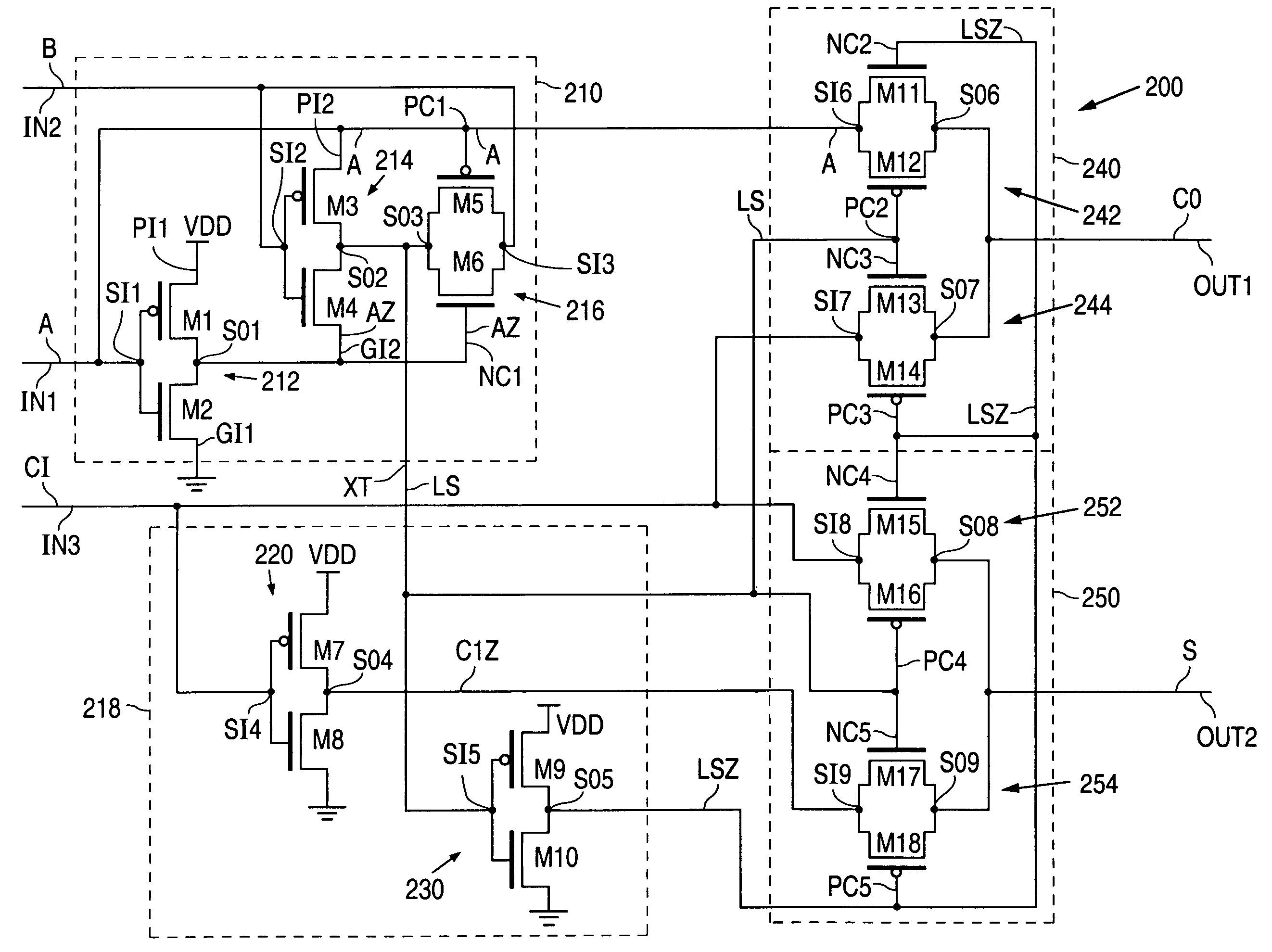
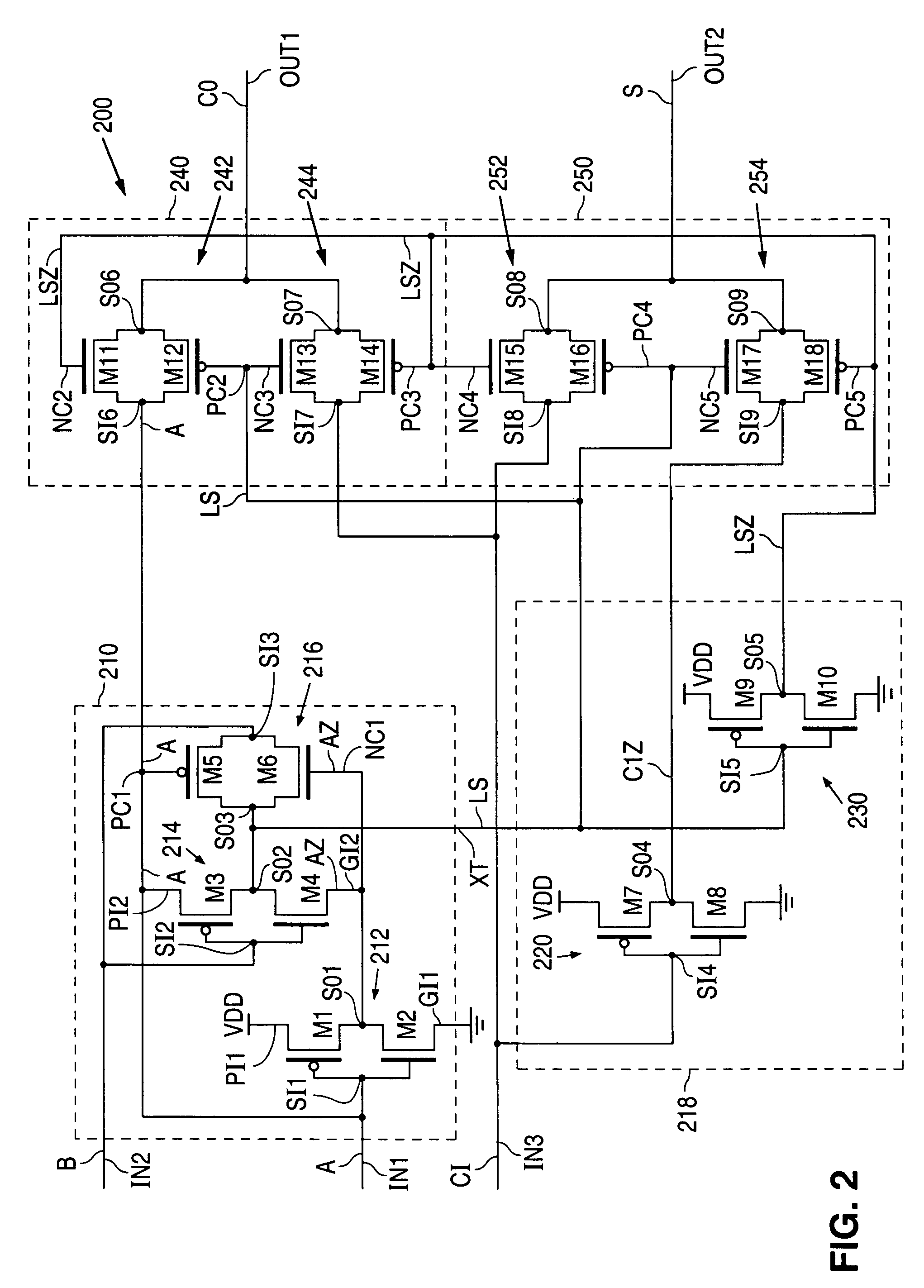
[0033]The adder cell further includes a carry output circuit which has a first control input connected to receive the logic signal, a second control input connected to receive the inverted first logic signal, and an output. The adder cell additionally includes a sum output circuit which has a first control input connected to receive the first logic signal, and a second control input connected to receive the inverted first logic signal. The sum output circuit also has a first sum input connected to the third input signal, a second sum input connected to the inverted third signal, and an output.

Problems solved by technology

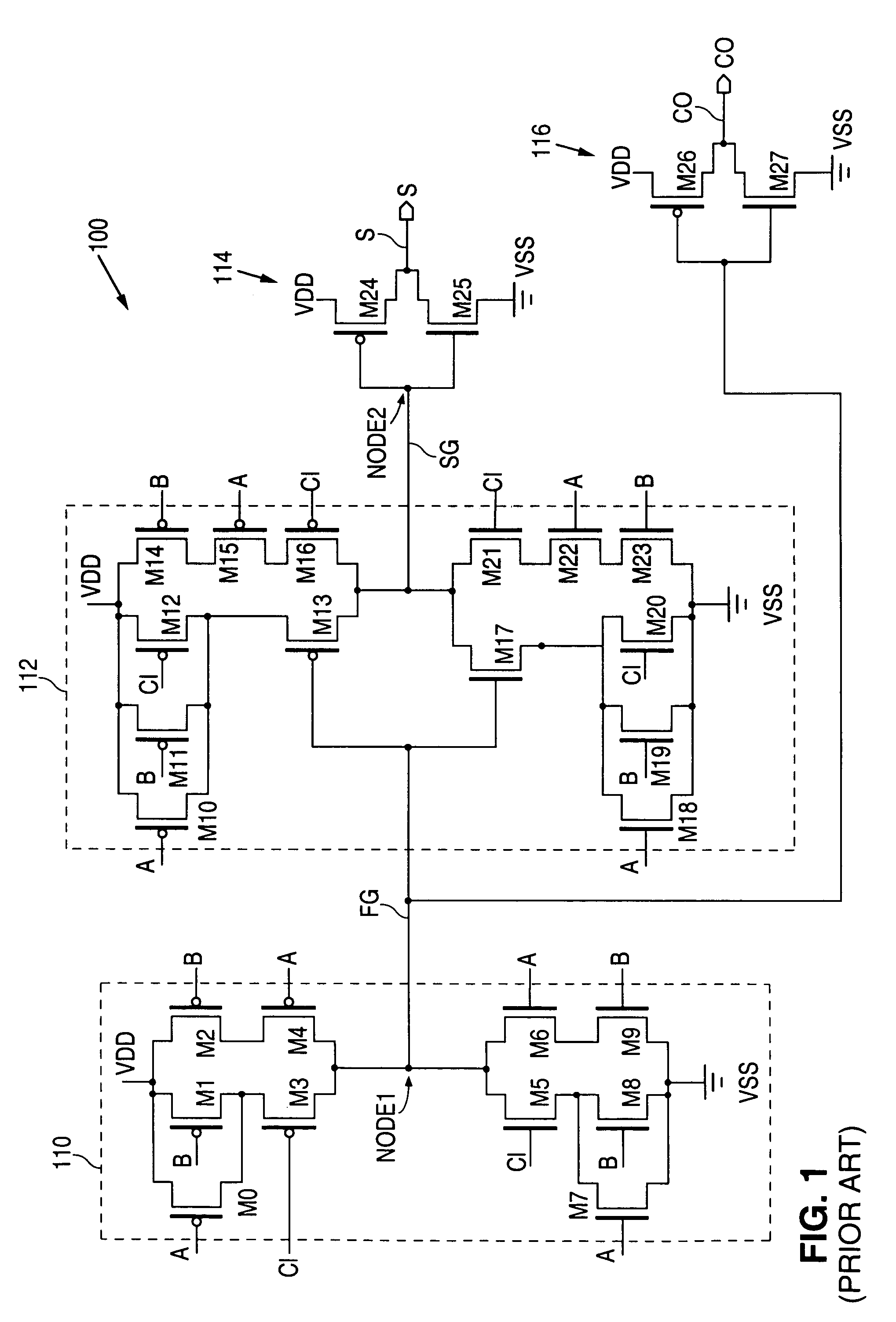
The high device count and the high device stacking are serious disadvantages because they increase the total gate capacitance, the total power dissipation and the total cell area.
Another disadvantage of full adder 100 is that its input / output signal polarity cannot be changed without adding inverters at the inputs / outputs of the adder.

Method used


Image

  • High speed, universal polarity full adder which consumes minimal power and minimal area
  • High speed, universal polarity full adder which consumes minimal power and minimal area
  • High speed, universal polarity full adder which consumes minimal power and minimal area

Examples


Embodiment Construction

[0048]In accordance with the present invention, FIG. 2 shows a schematic diagram illustrating a full adder cell 200. Full adder cell 200 has three inputs and two outputs. The three inputs include an adder input IN1 which receives a first input signal A, an adder input IN2 which receives a second input signal B, and an adder input IN3 which receives a third input signal CI. In addition, the two adder outputs include an output OUT1 which generates a carry output signal CO, and an output OUT2 which generates a sum output signal S.

[0049]As shown in FIG. 2, full adder cell 200 also includes an exclusive OR (XOR) gate 210 which has an output XT, a first input connected to adder input IN1, and a second input connected to adder input IN2. XOR gate 210 performs the XOR function based upon the logic states of input signals A and B on adder inputs IN1 and IN2. Thus XOR gate 210 generates an output signal LS on output XT in response to its A and B input signals.

[0050]Referring to FIG. 2, XOR ga...


PUM


Abstract

A low power, high speed full adder cell is described. This cell supports all possible combinations of active high / active low input / output signal polarity (32 different combinations), without adding extra inverters or extra transistors. The cell makes liberal use of complementary metal oxide semiconductor (CMOS) transmission gates in order to minimize the number of transistors used, and to minimize their stacking. This significantly decreases the total transistor gate area consumed, resulting in minimal power dissipation and minimal cell size.

Description

BACKGROUND OF THE INVENTION[0001]1. Field of the Invention[0002]The present invention relates to a full adder and, more particularly, to a high speed, universal polarity full adder which consumes minimal power and minimal area.[0003]2. Description of the Related Art[0004]Many applications require the use of high speed full adders which are low in power, small in size, and flexible with respect to the polarity (active high / active low) of their input / output signals. FIG. 1 shows the schematic diagram of a prior-art, transistor-based full adder cell 100.[0005]Referring to FIG. 1, it can be seen that full adder cell 100 includes two complex gates and two inverters: a first complex gate 110, a second complex gate 112, a first inverter 114 and a second inverter 116. First complex gate 110, which contains 10 transistors M0–M9, receives a first input signal A, a second input signal B, and a carry input signal CI. In addition, gate 110 also generates a first gate signal FG on node NODE1.[000...

Claims


Application Information

Patent Timeline
Patent Type & Authority Patents(United States)
IPC IPC(8): G06F7/50
CPCG06F7/501G06F2207/3872
Inventor PASQUALINI, RONALD
Owner NAT SEMICON CORP
Learn More