
Semiconductor device and method of manufacturing a semiconductor device

Active Publication Date: 2021-08-05
LAPIS SEMICON CO LTD
View PDF0 Cites 1 Cited by
  • Summary
  • Abstract
  • Description
  • Claims
  • Application Information

AI Technical Summary

Benefits of technology

The present patent aims to provide a semiconductor device and a manufacturing method that can prevent thermal stress-related failures. This is achieved by inhibiting the generation of thermal stress in the wiring layer of the device's circuit elements.

Problems solved by technology

This gives rise to the concern that the transistor characteristics may deteriorate.
Conventionally, when a temperature cycle test is performed on a printed circuit board on which a CSP has been mounted, there have been cases in which electrical characteristic defects have been generated.
However, wiring rules such as this are not sufficient countermeasures, and there have been cases in which characteristic variations have still occurred in spite of these countermeasures having been taken.
Furthermore, wiring rules such as this impose serious layout limitations when designing a CSP, and particularly in the case of current CSP which have an increasingly higher degree of integration, a basic solution to the above-described problem of thermal stress is still desired.

Method used


Image

  • Semiconductor device and method of manufacturing a semiconductor device
  • Semiconductor device and method of manufacturing a semiconductor device
  • Semiconductor device and method of manufacturing a semiconductor device

Examples


Embodiment Construction

[0020]Hereinafter, exemplary embodiments of the present disclosure will be described in detail with reference to the drawings. Note that in the following description, a mode in which a semiconductor device according to the present disclosure is applied to a CSP is described. Moreover, because the structure of the rewiring is similar to that of the conventional technology shown in FIG. 5, where necessary, reference will be made to FIG. 5 and a detailed description thereof will be omitted.

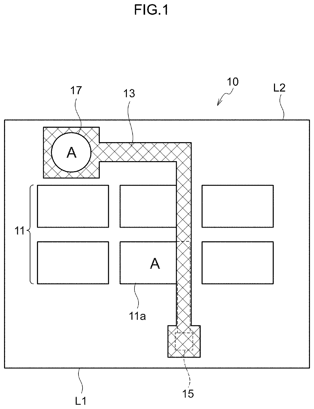
[0021]FIG. 1 shows a plan view of a rear surface of a semiconductor device 10 which is serving as a CSP. As is shown in FIG. 1, the semiconductor device 10 is formed so as to include a circuit element area 11, a pad 15, a terminal 17, and wiring 13 that connects the pad 15 and terminal 17 together. Note that, in FIG. 1, gaps 18 (described below) have been omitted from the drawings.

[0022]The circular element area 11 is an area where active devices such as transistors, diodes and the like, and passive ...


PUM


Abstract

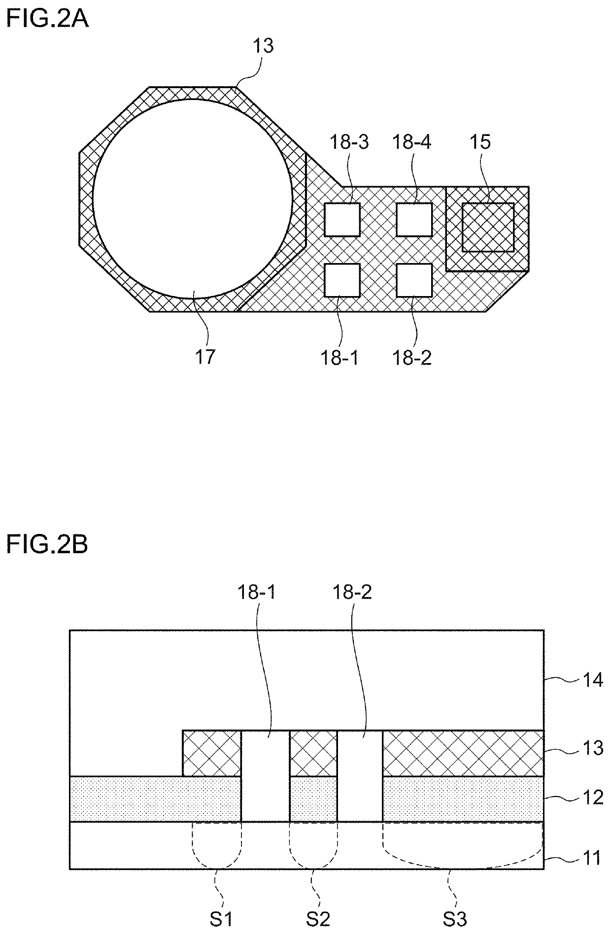
A semiconductor device includes wiring that is formed by a conductive body extending, via an insulating film, on a front surface of a semiconductor substrate, and an insulating layer that covers the front surface of the semiconductor substrate including the wiring. Gaps are provided extending from an upper surface of the wiring to a lower portion of the insulating film.

Description

CROSS-REFERENCE TO RELATED APPLICATION[0001]This application is based on and claims priority under 35 USC 119 from Japanese Patent Application No. 2020-017209 filed on Feb. 4, 2020, the disclosure of which is incorporated by reference herein.BACKGROUNDTechnical Field[0002]The present disclosure relates to a semiconductor device and to a method of manufacturing the semiconductor device.Related Art[0003]Conventionally, for example, Japanese Patent Application Publication Laid-Open (JP-A) NO. 2000-183214 is known as a publication concerned with the problem of stress generated in wiring. JP-A No. 2000-183214 describes how, in a chip-size package (hereinafter, referred to as a CSP), in an environment of a temperature cycle test or the like when the CSP is being packaged, the Cu wiring becomes synergistic with the metal posts and sizable stress is applied to the LSI transistor directly underneath this Cu wiring. This gives rise to the concern that the transistor characteristics may deteri...

Claims


Application Information

Patent Timeline
IPC IPC(8): H01L23/00
CPCH01L24/02H01L24/05H01L24/13H01L2224/13024H01L2224/02373H01L2224/05008H01L2224/02311H01L24/03H01L2224/0231H01L2224/0233H01L2224/0237H01L2224/02351H01L2224/0235H01L2224/02375H01L2224/05569H01L2224/0401H01L2224/0346H01L2224/0347H01L2224/024H01L2224/131H01L2924/00014H01L2924/014
Inventor SHINDO, MASANORI
Owner LAPIS SEMICON CO LTD
Learn More