
Solid-state electronic circuit, image pickup element, method of controlling image pickup element, and electronic device

Pending Publication Date: 2021-08-05
SONY SEMICON SOLUTIONS CORP
View PDF0 Cites 0 Cited by
  • Summary
  • Abstract
  • Description
  • Claims
  • Application Information

AI Technical Summary

Benefits of technology

The patent aims to prevent failures and increase yields. The technical effect of the patent is to improve the efficiency and accuracy of manufacturing processes.

Problems solved by technology

However, in a case where provided is a system having such a circuit configuration, the circuit-layout density rises rapidly along with an increase in the number of pixels, resulting in an increase in the probability of occurrence of circuit failure causing, for example, code failure.
Furthermore, in a case where failure has occurred in pixel data particularly in a solid-state image pickup device, even if the failure is a 1-bit failure, the occurrence of the failure disables the function of the chip, resulting in a deterioration in yield.

Method used


Image

  • Solid-state electronic circuit, image pickup element, method of controlling image pickup element, and electronic device
  • Solid-state electronic circuit, image pickup element, method of controlling image pickup element, and electronic device
  • Solid-state electronic circuit, image pickup element, method of controlling image pickup element, and electronic device

Examples


Embodiment Construction

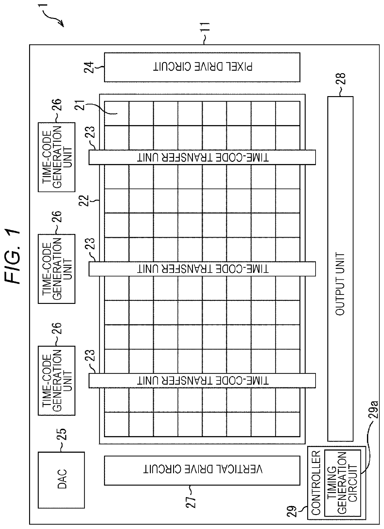
[0048]A preferred embodiment of the present disclosure will be described in detail below with reference to the accompanying drawings. Note that, in the present specification and the drawings, constituent elements having substantially the same functional configurations are denoted with the same reference signs, and thus the duplicate descriptions thereof will be omitted.

[0049]Furthermore, the descriptions will be given in the following order.

[0050]1. Exemplary Schematic Configuration of Solid-State Image Pickup Device

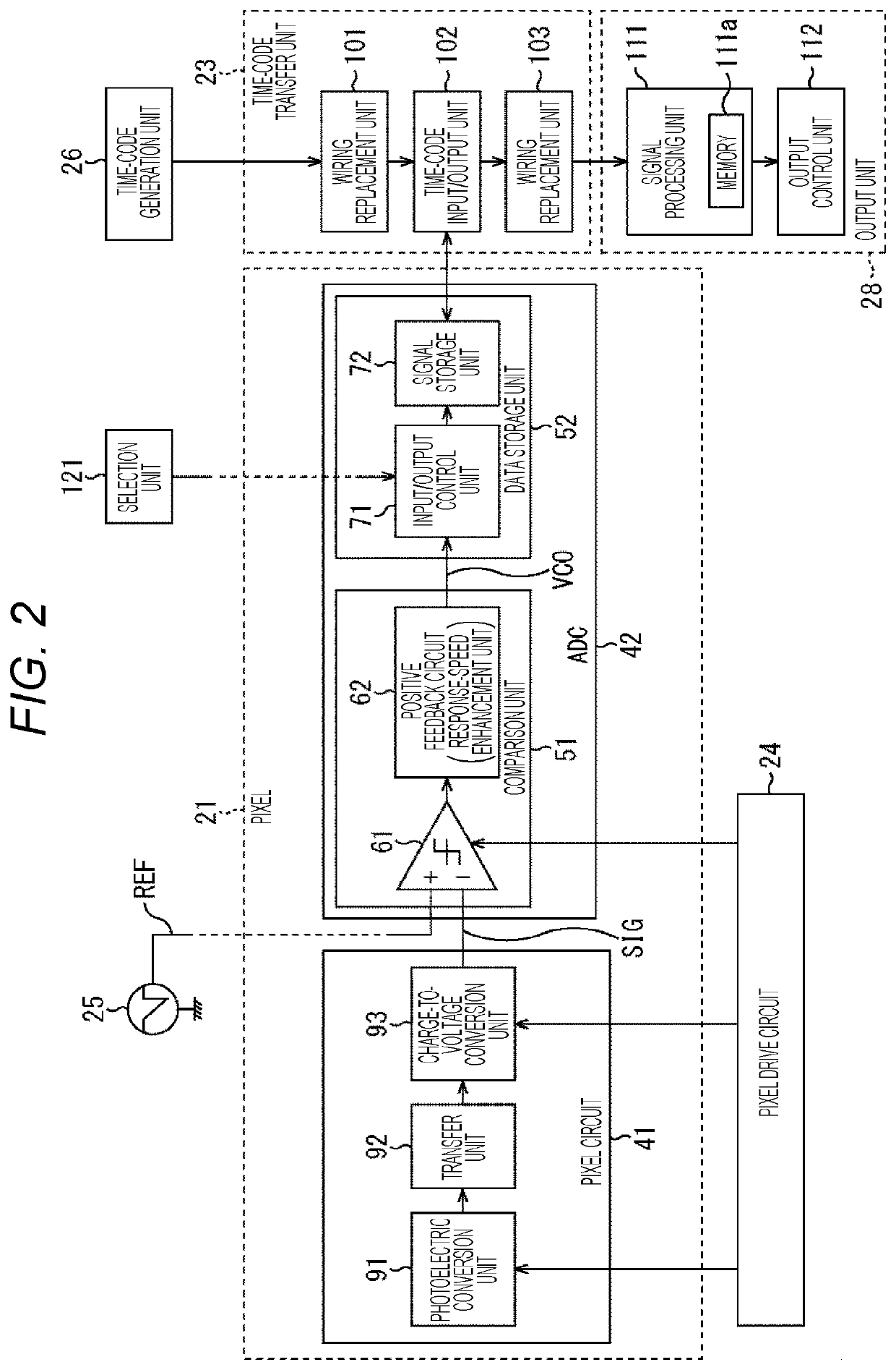
[0051]2. Exemplary Detailed Configuration of Pixel

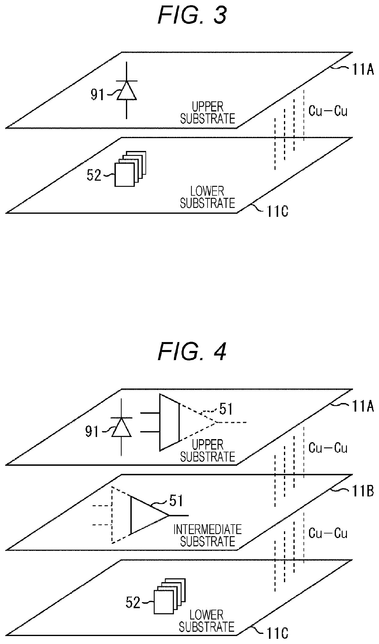
[0052]3. Multiple-Substrate Configuration 1

[0053]4. Multiple-Substrate Configuration 2

[0054]5. Sectional Structure of Pixel

[0055]6. Exemplary Circuit Configuration of Pixel

[0056]7. Exemplary Circuit Configuration of Time-Code Input / Output Unit

[0057]8. Detailed Configuration for Controlling Time-Code Transfer Units

[0058]9. Exemplary Detailed Configurations of Wiring Replacement Units

[0059]10. Exemplary Specific Operation o...


PUM


Abstract

The present disclosure relates to a solid-state electronic circuit, an image pickup element, a method of controlling the image pickup element, and an electronic device that enable inhibition of a deterioration in yield due to densification of image pickup elements.Wiring replacement units are provided between a plurality of transfer paths allowing bitwise transfer of a predetermined bit length of time code for use in conversion of a pixel signal corresponding to a quantity of light received in a pixel into a digital signal. In a case where an error has occurred in any of the plurality of transfer paths, replacement with the transfer path lowest in priority is performed. The present disclosure can be applied to image pickup elements.

Description

TECHNICAL FIELD[0001]The present disclosure relates to a solid-state electronic circuit, an image pickup element, a method of controlling the image pickup element, and an electronic device. The present disclosure relates particularly to a solid-state electronic circuit, an image pickup element, a method of controlling the image pickup element, and an electronic device that enable an improvement in yield.BACKGROUND ART[0002]As a mode advantageous in area efficiency in a case where analog digital (AD) conversion is performed in a limited area, such as in a pixel, in the signal readout mode of an image pickup element, there is a proposed integrating (slope) AD conversion mode with a comparator and a digital circuit at the post stage to the comparator.[0003]As technology for achievement of AD conversion in a limited area with the integrating AD conversion mode, for example, there is a widely known circuit configuration in which one dynamic random access memory (DRAM) circuit is provided...

Claims


Application Information

Patent Timeline
IPC IPC(8): H04N5/3745H04N17/00H04N5/374
CPCH04N5/3745H04N5/378H04N5/3742H04N17/002H04N25/772H04N25/75H04N25/77H04N25/767
Inventor SAKAKIBARA, MASAKI
Owner SONY SEMICON SOLUTIONS CORP
Learn More