
Method of manufacturing microelectronic components

Pending Publication Date: 2022-03-03
COMMISSARIAT A LENERGIE ATOMIQUE ET AUX ENERGIES ALTERNATIVES
View PDF0 Cites 0 Cited by
  • Summary
  • Abstract
  • Description
  • Claims
  • Application Information

AI Technical Summary

Benefits of technology

The patent text describes a way to remove metal residues without affecting fully formed silicidated portions. This prevents or limits the deposition of unwanted metal residues and eliminates the need for cleaning the metal residues.

Problems solved by technology

The gaps become difficult to fill completely.
They can have negative consequences for CMOS circuits.
During the subsequent formation of the electrical contacts at the silicided portions, and in particular when a problem with the alignment of these electrical contacts arises, the voids can be opened and filled with metal.
However, this solution has other drawbacks, in particular in that it affects the other portions of the transistors, in particular the silicided portion, the semiconductor material of the active areas or the STIs.
This can further damage the STIs 30.
This can also consume or damage part of the silicided portions.

Method used


Image

  • Method of manufacturing microelectronic components
  • Method of manufacturing microelectronic components
  • Method of manufacturing microelectronic components

Examples


first embodiment

[0131]The first embodiment is shown in FIG. 9A to 9C. FIG. 9A shows a sectional view of two adjacent gates flanked by the first spacers 11 a and the second spacers 11b, prior to the silicidation of the upper portions 121, FIG. 9B shows the positioning of the step of removing the second spacers 11b, also known as SPT (Spacer Proximity Technology), in the sequence of steps of the NiSi module, FIG. 9C shows a sectional view of two adjacent gates flanked by the first spacers 11a and comprising silicided portions 12, as obtained at the end of the NiSi module modified by the SPT step.

[0132]According to this first embodiment, the removal of the second spacers 11b is carried out at the very beginning of the NiSi module, before the “deposition preparation” step. Such a “deposition preparation” step is generally aimed at removing native oxide and / or impurities, for example of the organic or metallic type, at the tip of the gates and / or the sources and drains. It can comprise at least one prep...

second embodiment

[0134]The second embodiment is shown in FIG. 10A to 10C. FIG. 10A shows a sectional view of two adjacent gates flanked by the first spacers 11a and the second spacers 11b, prior to the silicidation of the upper portions 121. FIG. 10B shows the positioning of the SPT step in the sequence of steps of the NiSi module. FIG. 10C shows a sectional view of two adjacent gates flanked by the first spacers 11 a and comprising silicided portions 12, as obtained at the end of the NiSi module modified by the SPT step.

[0135]According to this second embodiment, the removal of the second spacers 11b takes place immediately after the “deposition preparation” step, before the NiPt deposition step.

[0136]The NiPt deposition can typically comprise, prior to the actual deposition, a prior soft etching aiming at removing any remaining contaminants and ensure that no interfacial oxide is present prior to deposition. This prior soft etching can be carried out via a SiCoNi™-type method.

[0137]The SPT can take...

third embodiment

[0138]The third embodiment is shown in FIG. 11A to 11C. FIG. 11A shows a sectional view of two adjacent gates flanked by the first spacers 11a and the second spacers 11b, prior to the silicidation of the upper portions 121. FIG. 11B shows the positioning of the SPT step in the sequence of steps of the NiSi module. FIG. 11C shows a sectional view of two adjacent gates flanked by the first spacers 11 a and comprising silicided portions 12, as obtained at the end of the NiSi module modified by the SPT step.

[0139]According to this third embodiment, the removal of the second spacers 11b takes place before the “thermal anneal 2” step, preferably immediately after the “partial NiPt removal” step. The thermal anneal 2 can be rapid thermal annealing known as RTA or laser annealing. The thermal anneal 2 in particular allows the diffusion and reaction of the nickel in the upper portions 121 to be finalised so as to obtain the silicided portions 12. The SPT can take place with the different etc...


PUM


Abstract

A method is provided for producing a plurality of transistors on a substrate comprising at least two adjacent active areas separated by at least one electrically-isolating area, each transistor of the plurality of transistors including a gate having a silicided portion, and first and second spacers on either side of the gate, the first spacers being located on sides of the gate and the second spacers being located on sides of the first spacers. The method includes forming the gates of the transistors, forming the first spacers, forming the second spacers siliciding the gates so as to form the silicided portions of the gates, and removing the second spacers. The removal of the second spacers takes place during the silicidation of the gates and before the silicided portions are fully formed.

Description

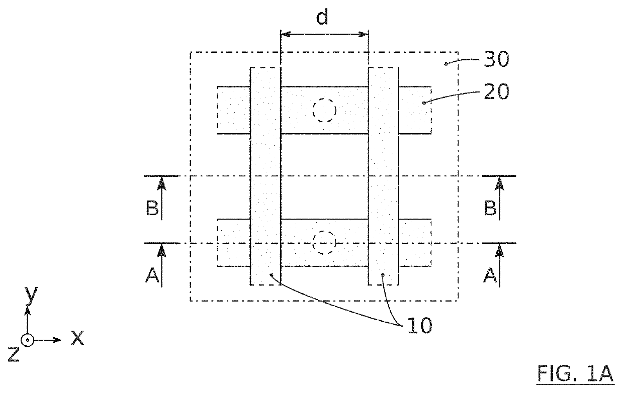
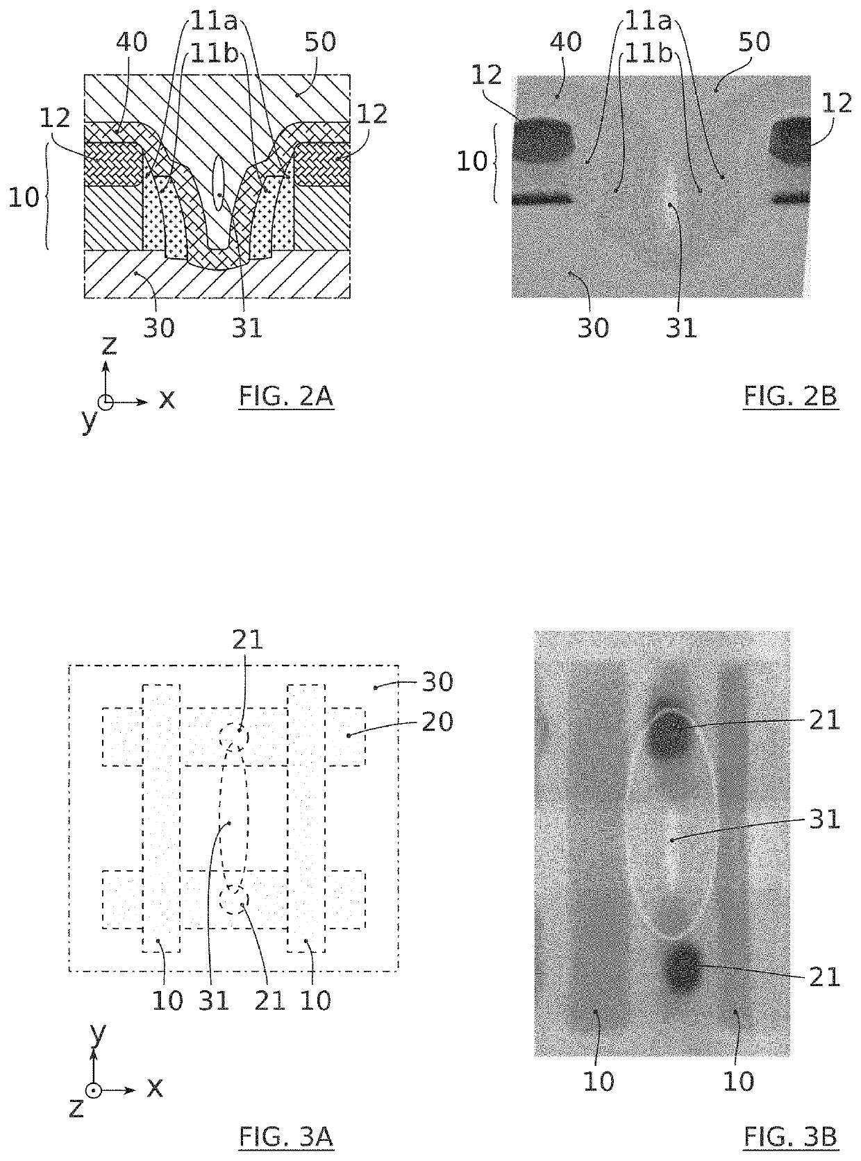
TECHNICAL FIELD[0001]The present invention relates to the field of manufacturing microelectronic components. It advantageously applies to the manufacture of CMOS transistors (Complementary Metal-Oxide-Semiconductor transistors), however it is not limited thereto.PRIOR ART[0002]A conventional layout of transistors in a CMOS circuit is shown in FIG. 1A. The gates 10 of the transistors typically extend transversally across a plurality of active areas 20, In order to electrically separate the different active areas 10, for example p-type and n-type areas, shallow isolating trenches STI 30 (shallow trench isolation) are usually formed,[0003]In order to increase the overall performance of a CMOS circuit, the transistors are integrated in an increasingly dense layout. The distance d between two adjacent gates 10 is thus reduced to a minimum. In order to increase the performance of individual transistors, compressive or tensile films, also known as “stress liners” (for example CESL: “Contac...

Claims


Application Information

Patent Timeline
IPC IPC(8): H01L21/8238H01L27/092H01L29/49H01L21/02H01L21/28H01L21/311H01L29/66
CPCH01L21/823835H01L27/092H01L29/4933H01L21/02068H01L29/6653H01L21/31116H01L21/823864H01L29/6656H01L21/28052H01L21/823443H01L21/823468H01L29/665
Inventor NEMOUCHI, FABRICEFITZ, CLEMENSPOSSEME, NICOLAS
Owner COMMISSARIAT A LENERGIE ATOMIQUE ET AUX ENERGIES ALTERNATIVES
Learn More