Bipolar transistor stabilized with electrical insulating elements

Inactive Publication Date: 2000-02-29
THOMSON CSF SA
View PDF15 Cites 31 Cited by
  • Summary
  • Abstract
  • Description
  • Claims
  • Application Information

AI Technical Summary

Problems solved by technology

The problem of this type of structure however lies in their poor stability inasmuch as the diffusion achieved for

Method used


Image

  • Bipolar transistor stabilized with electrical insulating elements
  • Bipolar transistor stabilized with electrical insulating elements
  • Bipolar transistor stabilized with electrical insulating elements

Examples


Embodiment Construction

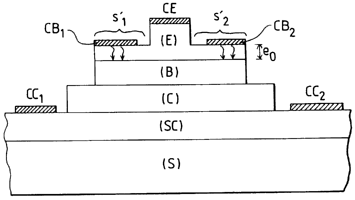
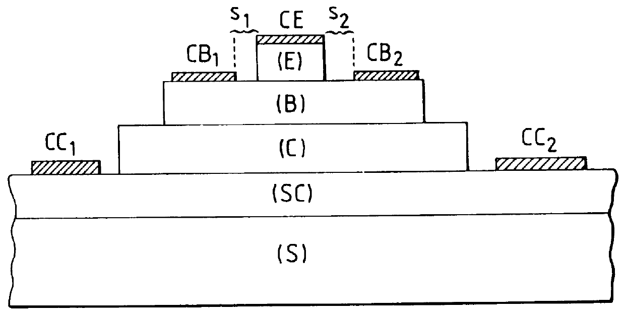
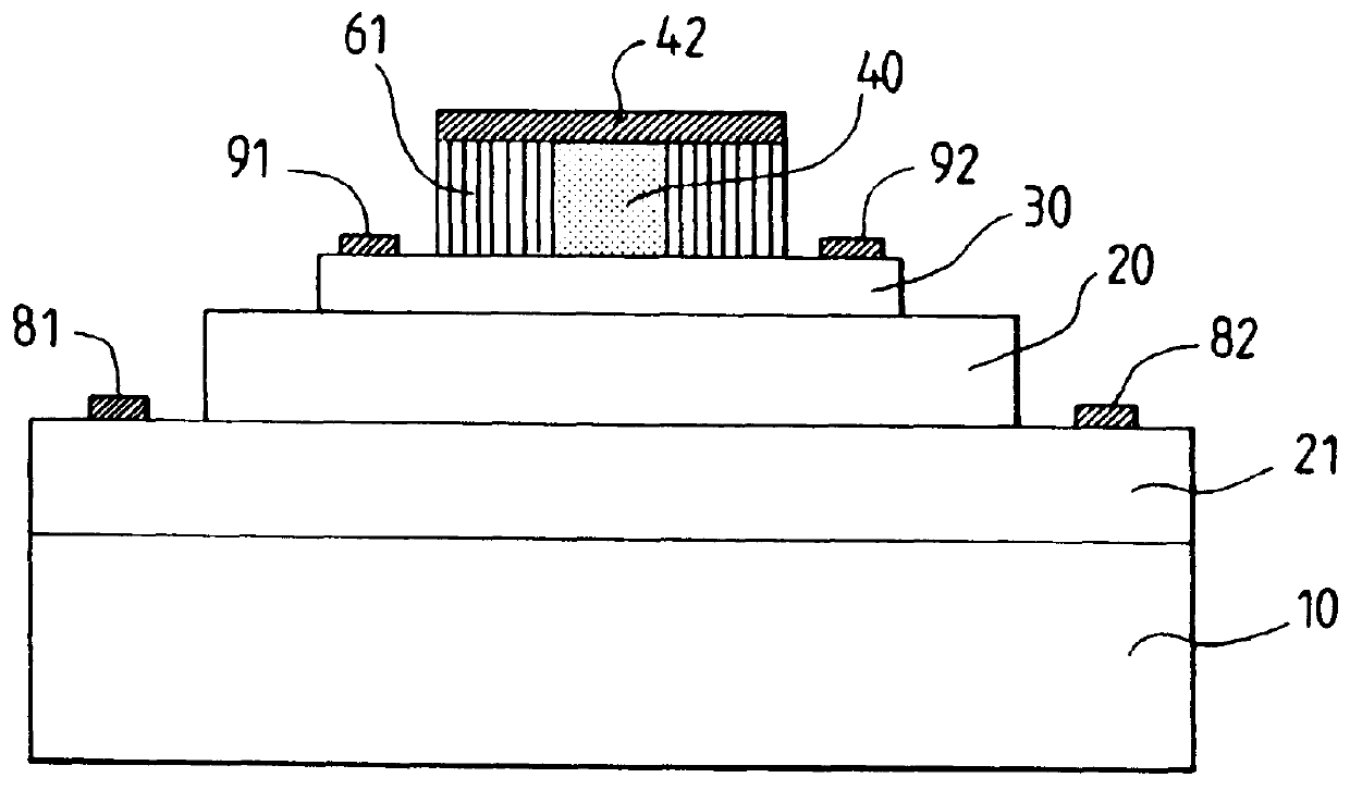
The heterojunction bipolar transistor according to the invention is shown schematically in FIG. 3, in the case of a structure with the emitter at the top (it must be noted that the invention can also be applied to the case of a structure with a collector at the top). The bipolar transistor according to the invention comprises a substrate 10, a sub-collector 21, a collector 20, a base 30 and an emitter 40. Ohmic contacts 81 and 82 of the collector are located on the sub-collector layer 21, base ohmic contacts 91, 92 are located on the base on either side of the emitter mesa 40 whose flanks are in contact with electrical insulating elements 61. An emitter ohmic contact 42 is located on the entire mesa 40 and the insulating elements 61.

The invention shall be described more specifically in the context of Ga.sub.0.5 In.sub.0.5 P / GaAs, npn doped heterojunction bipolar transistors. The choice of a phosphorus-based material and an arsenic-based material provides for behavior with respect to...


PUM


Abstract

A semiconductor component of the heterojunction bipolar transistor type comprises, on a substrate, a collector, a base and a mesa-shaped emitter resting on the base. The bipolar transistor furthermore comprises electrically insulating elements in contact with the base and the flanks of the emitter mesa, said elements having a width of the same magnitude as the width of the mesa and providing the component with greater stability. Furthermore, a method for the manufacture of a component of this kind comprises in particular a step for the ion implantation of insulating ions through the constituent layer of the emitter mesa so as to define the electrically insulating elements.

Description

1. Field of the InventionThe field of the invention is that of bipolar transistors and especially vertical structure heterojunction bipolar transistors in which the current is conveyed perpendicularly to the surface of the substrate. These transistors are used for microwave applications.A bipolar transistor is constituted by a stack of layers of semiconductor materials, of which at least one surface layer is etched in a mesa formation, namely a raised or embossed pattern. FIG. 1 illustrates a standard structure of a heterojunction bipolar transistor or HBT comprising a substrate S, a sub-collector SC, a collector C, a base B and an emitter E. Conventionally, a contact CE is made on the surface of the emitter by the superimposition of matched layers. Laterally, two contacts CB.sub.1 and CB.sub.2 are also made in the collector on either side of the base.This type of vertical structure raises a problem of electron / hole recombination at the free surfaces S.sub.1 and S.sub.2 shown in FIG...

Claims


Application Information

Patent Timeline
IPC IPC(8): H01L23/34H01L29/08H01L21/02H01L29/02H01L23/367H01L29/737H01L21/331H01L29/66H01L29/73H01L29/205
CPCH01L23/367H01L29/0817H01L29/66318H01L29/7371H01L2924/0002H01L2924/00
Inventor DELAGE, SYLVAINCASSETTE, SIMONEHENKEL, ACHIMSALZENSTEIN, PATRICE
Owner THOMSON CSF SA
Why Eureka
Try Eureka