
Apparatus for producing semiconductors and other devices and cleaning apparatus

Inactive Publication Date: 2000-03-14
ALPS ALPINE CO LTD
View PDF22 Cites 78 Cited by
  • Summary
  • Abstract
  • Description
  • Claims
  • Application Information

AI Technical Summary

Problems solved by technology

In the above apparatus, however, the substrates held in the transfer means MTV are exposed to the atmosphere in a clean room after being cleaned.
Exposure to the atmosphere causes impurities to adhere to the substrate surfaces even in the clean room.
If film deposition is performed on the substrates with impurities kept adhered to their surfaces, the quality of the deposited films may deteriorate and the yield of the produced devices may reduce.
An improvement in film quality resulted with the related art (2) is, however, not so satisfactory as expected.

Method used


Image

  • Apparatus for producing semiconductors and other devices and cleaning apparatus
  • Apparatus for producing semiconductors and other devices and cleaning apparatus
  • Apparatus for producing semiconductors and other devices and cleaning apparatus

Examples


Embodiment Construction

)

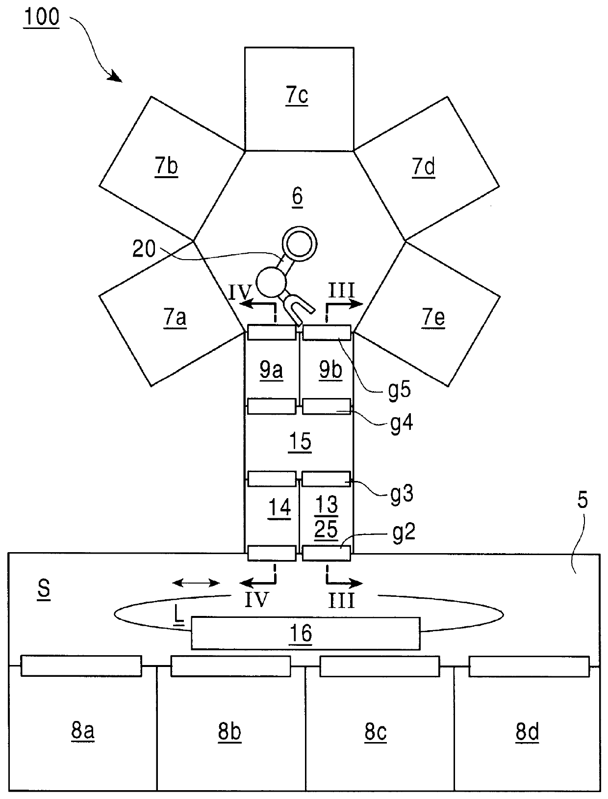
The following test was made by using the apparatus for producing semiconductor and other devices, shown in FIG. 1.

Substrates for liquid crystal display devices, which include silicon films formed on their surfaces, were prepared as a sample a, a sample b, a sample c, and a sample d.

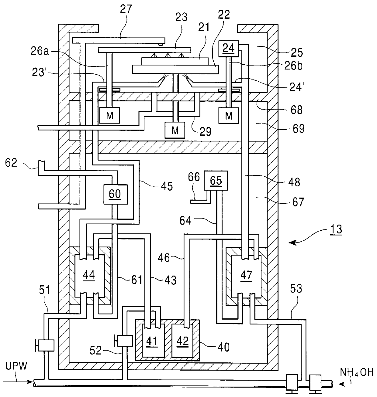
On the other hand, ozonized water and hydrogenated water were produced on the following conditions by using the cleaning apparatus shown in FIG. 2.

(Conditions for Producing Hydrogenated Water and Ozonized Water)

voltage.apprxeq.3[V]

current.apprxeq.35[A]

a mount of ozone gas generated.apprxeq.1.3[g / hr]

amount of hydrogen gas generated.apprxeq.1.3[g / hr]

ozonized water

(a) 6[ppm], 2 [1 / min]

(b) ORP.apprxeq.1270[mV] vs [NHE]

(c) pH.apprxeq.6.3

hydrogenated water

(a) 1.2[ppm], 2 [1 / min]

(b) ORP.apprxeq.-630[mV] vs [NHE]

(c) pH.apprxeq.10

* ORP: oxidizing / reducing potential

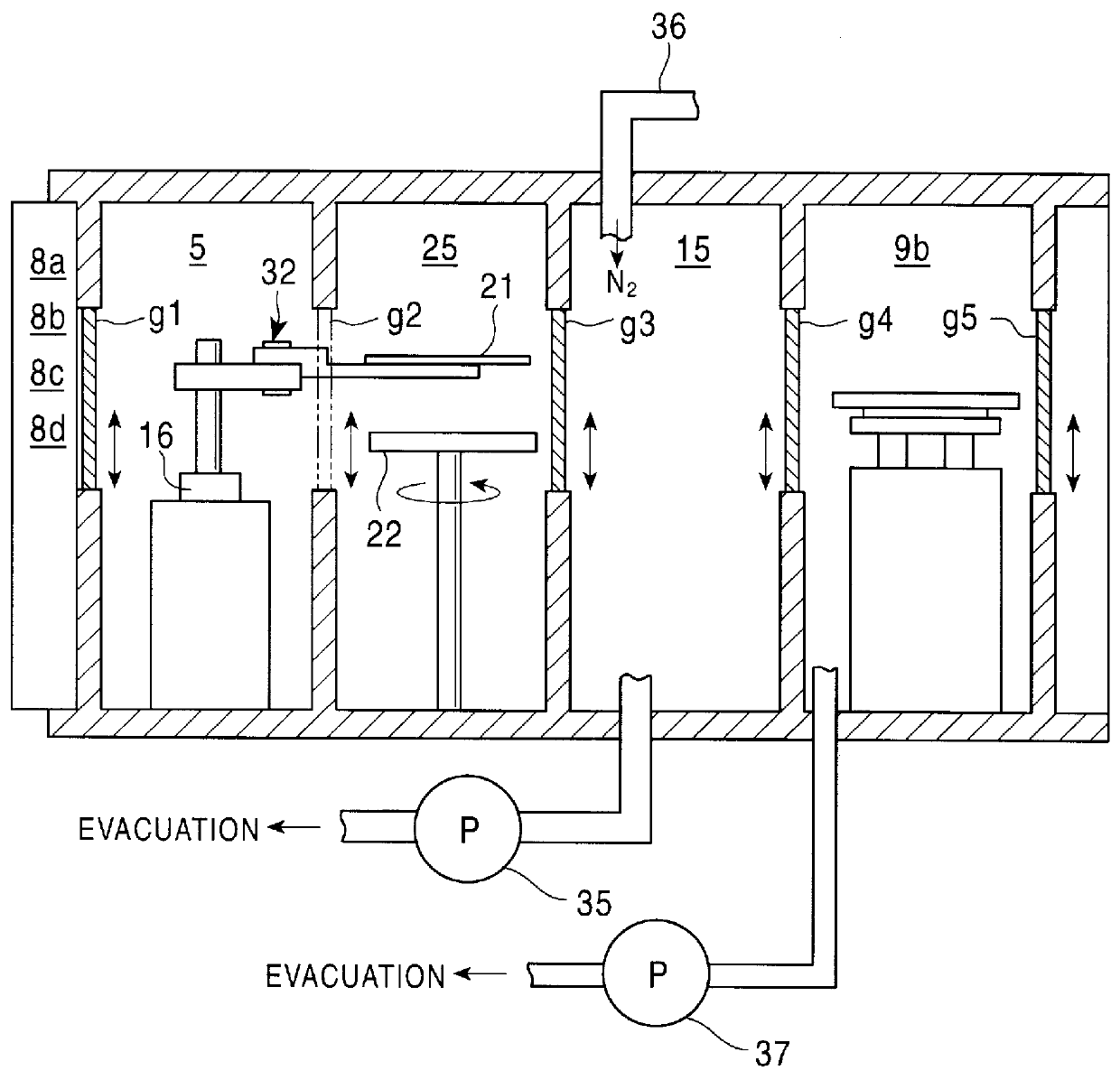
The substrate for a liquid crystal display device, prepared as the sample a, was carried into the cleaning apparatus 13 via the loading / unloading chamb...


PUM


Abstract

Provided is an apparatus for producing semiconductor and other devices, which can improve the quality of deposited films and increase the yield of produced devices in comparison with the conventional apparatus. The apparatus of the invention comprises a plurality of dry treatment chambers (7a, 7b, 7c, 7d, 7e), a transfer room (6) interconnecting the dry treatment chambers (7a, 7b, 7c, 7d, 7e), loading / unloading chambers (8a, 8b, 8c, 8d), and a cleaning apparatus (13). The transfer room (6) and the cleaning apparatus (13) are directly or indirectly connected to each other.

Description

1. Field of the InventionThe present invention relates to an apparatus for producing semiconductor and other devices, and more particularly to an apparatus for performing film deposition, etching, etc. on semiconductors and so on (e.g., semiconductors, magnetic substances, conductors, dielectrics and other materials).2. Description of the Related Art(1) An apparatus for producing semiconductor and other devices, shown in FIG. 10, has been known heretofore.Semiconductor substrates are cleaned in a cleaning apparatus 1 and then stocked in a carrier 215 (FIG. 11) disposed in a transfer means MTV.Upon a predetermined number of substrates being stocked in the carrier 215, the carrier 215 including those substrates is carried by the transfer means MTV into any of loading / unloading chambers 8a, 8b, 8c, 8d of the apparatus for producing semiconductor and other devices.The semiconductor substrates having entered any of the loading / unloading chambers 8a, 8b, 8c, 8d are loaded into standby roo...

Claims


Application Information

Patent Timeline
IPC IPC(8): B08B3/02H01L21/00C02F1/46H01L21/304H01L21/677
CPCB08B3/02H01L21/67161H01L21/67167H01L21/67207H01L21/67745Y10S134/902
Inventor EUI-YEOL, OH
Owner ALPS ALPINE CO LTD
Learn More