
Eureka
For R&D, Eureka makes reading and utilizing patents & technical documents easy.
Eureka AIR
Designed for self-driven R&D workflows. Generate viable solutions, solve complex R&D challenges, empower your innovation with AI.

Eureka Materials
Designed for material experts only. Revolutionize your material R&D, from search, analyze, to developing new materials.

TechResearch
Generate reliable direction feasibility study reports for your R&D in just a few steps.

TechSeek
Discover and master advanced knowledge NOW. Basics, ideas, possibilities, all at once.

TechMind
As an expert in R&D Theories, TechMind can generates customized viable solutions instantly.

TechRisk
Analyze your overall solution with one click, know your potential R&D risks in advance.

TechMonitor
Get weekly tech updates, stay abreast of the latest tech innovations and key insights.
Liquid crystal apparatus and driving method therefor
- Summary
- Abstract
- Description
- Claims
- Application Information
AI Technical Summary
Problems solved by technology
Method used
Image

Examples
second example
In this example, the liquid crystal panel of the first example was modified in the following manner while the electrodes and polarizers were disposed in the same manner.
One of a pair of substrates 302 was coated with a ca. 10 nm-thick polyimide film 306 and rubbed in one direction with nylon cloth, and the other substrate was subjected to a homeotropic aligning treatment by application of a silane coupling agent (ODS-E). The two substrates were superposed each other with silica beads of 2.0 .mu.m in average diameter disposed therebetween and bonded to each with a sealing agent.
The cell gap was filled with a ferroelectric liquid crystal showing the following properties and exhibiting a bent-free so-called bookshelf layer structure instead of a chevron layer structure when incorporated in the above-prepared panel.
Phase transition series (.degree. C.) ##STR2## Spontaneous polarization Ps=30 nC / cm.sup.2 (30.degree. C.) Tilt angle H=20 deg. (30.degree. C.)
Dielectric anisotropy .DELTA..ep...
second embodiment
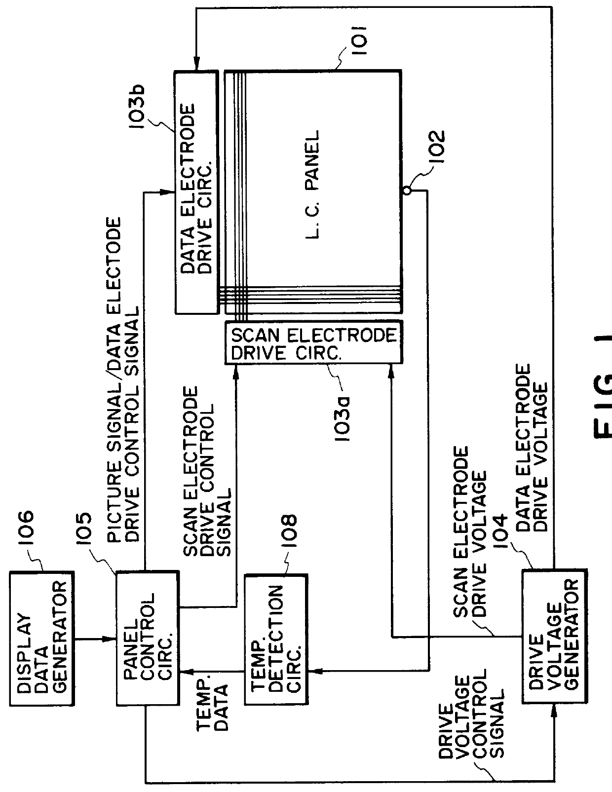
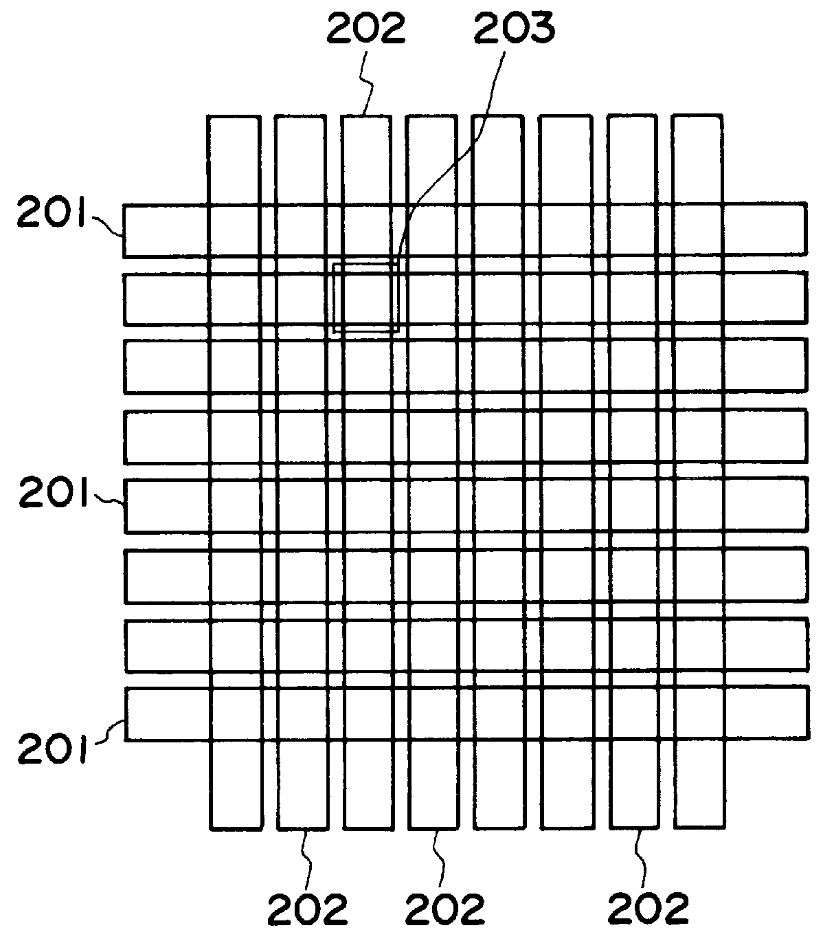
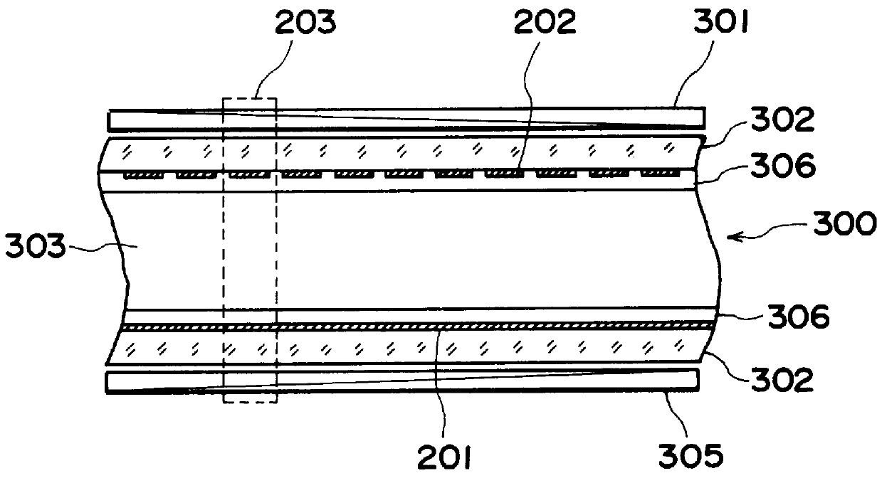
This embodiment uses an entire apparatus structure as shown in FIG. 1, and a liquid crystal panel structure as shown in FIGS. 2 and 3 similarly as the first embodiment described above, but an anti-ferroelectric liquid crystal assuming three stable states is used and subjected to multiplex drive by using a set of drive waveforms as shown in FIG. 6 while controlling the drive voltage Vop and selection period according to a temperature compensation scheme similarly as shown in FIG. 5 except for specific value shown therein.
More specifically, referring to FIG. 6, a scanning signal (S1, S2, . . . ) is composed of a reset portion R, a selection portion S and a non-selection portion NS. In the non-selection period NS, an offset voltage is applied. The scanning signal may be polarity-inverted frame by frame as shown. Vop refers to a voltage applied to the liquid crystal in a selection period at S1-I. In this embodiment, in applying the temperature compensation scheme as shown in FIG. 1, plu...
third embodiment
This embodiment uses an entire apparatus structure as shown in FIG. 1 and a liquid crystal panel structure as shown in FIGS. 2 and 3, similarly as the first embodiment, but a liquid crystal material showing a bistable twisted nematic mode is used. In this embodiment, a drive waveform as shown in FIG. 7 (and disclosed in JP-A 6-230751) may be used. When the drive waveform shown in FIG. 7 is used, nematic liquid crystal molecules are caused to stand up by application of a prescribed voltage in period T1 and then caused to select between a 2.pi.-twisted state (in case of application of a voltage below a threshold voltage) and a non-twisted state (in case of application of a voltage exceeding a threshold voltage), thereby determining a "black" or a "white" display state. During the drive, the drive voltage Vop and selection period 1H may be controlled according to a temperature compensation scheme similarly as shown in FIG. 5 except for specific values shown therein. Also in this embodi...
PUM
 Abstract
Description
Claims
Application Information
 - R&D Engineer
- R&D Manager
- IP Professional
- Industry Leading Data Capabilities
- Powerful AI technology
- Patent DNA Extraction
Browse by: Latest US Patents, China's latest patents, Technical Efficacy Thesaurus, Application Domain, Technology Topic, Popular Technical Reports.
© 2024 PatSnap. All rights reserved.Legal|Privacy policy|Modern Slavery Act Transparency Statement|Sitemap|About US| Contact US: help@patsnap.com