

Structure for an antifuse cell
a structure and anti-fuse technology, applied in the direction of semiconductor devices, semiconductor/solid-state device details, electrical apparatus, etc., can solve the problems of anti-fuse element shortening, anti-fuse dielectric damage, and the etching process tends to undercut the polysilicon
- Summary
- Abstract
- Description
- Claims
- Application Information
AI Technical Summary
Problems solved by technology
Method used
Image

Examples
Embodiment Construction
It will be appreciated that the present invention can take many forms and embodiments. Some embodiments of the invention are described so as to give an understanding of the invention. It is not intended, however, that the embodiments of the present invention that are described in this specification should limit the invention.
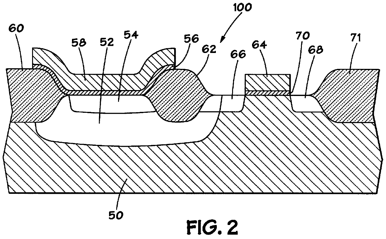
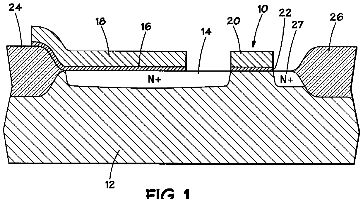
Before discussing embodiments of the present invention, it is appropriate to consider the structure of prior art antifuse cells. With reference therefore to FIG. 1, there is shown the structure of an antifuse cell according to the prior art. The bottom plate of the antifuse element is N+ region 14, while the top plate is polysilicon layer 18. Interposed between those two plates is a dielectric 16, which may, for example, be an ONO dielectric composed of a native oxide layer, a silicon nitride layer and an upper oxide layer. The N+ region 14 is contiguous with and forms the source of access transistor 10. The drain of access transistor 10 comprises N+ region 27, ...
PUM
 Abstract
Description
Claims
Application Information