Flip chip mounting method and semiconductor apparatus manufactured by the method

a technology of mounting method and semiconductor apparatus, which is applied in the direction of electrical apparatus, semiconductor device details, semiconductor/solid-state device devices, etc., can solve the problems of insufficient electrical and mechanical bonding capability of acp, insufficient high-quality eutectic metal formation, and conventional technique not providing a high-level stable and reliable mounting method

Inactive Publication Date: 2000-10-24
SEIKO EPSON CORP
View PDF3 Cites 76 Cited by
  • Summary
  • Abstract
  • Description
  • Claims
  • Application Information

AI Technical Summary

Problems solved by technology

Further, in the case of an ACP, electrical and mechanical bonding capability of the ACP may not be sufficient.
The conventional technique therefore does not provide a high level of stable and reliable mounting method.
Also, when the metal eutectic reaction between bumps on the IC chip and metal on the substrate surface is used, good quality eutectic metal is not formed and poor bonding takes place if there is even a small defect in the finishing of the bumps or the metal surface.
As a result, when the IC chip is bonded to the substrate, the paste-like adhesive having a high fluidity instantaneously fills gaps between the surface of the IC chip on which the electrode is formed and the ACF, and therefore bubbles are not readily generated.
Further, when bumps are provided on the IC chip, there may be an occasion where the ACF cannot conform itself to changes in the surface configuration of the IC chip in an area adjacent to the bumps, bubbles may remain in the area adjacent the bumps.
As a result, when the IC chip and the substrate are bonded together, air is difficult to remain between the IC chip and the substrate.
Furthermore, a washing step to remove remained flux becomes unnecessary.

Method used


Image

  • Flip chip mounting method and semiconductor apparatus manufactured by the method
  • Flip chip mounting method and semiconductor apparatus manufactured by the method
  • Flip chip mounting method and semiconductor apparatus manufactured by the method

Examples


Embodiment Construction

Hereunder, embodiments of a flip chip mounting method and a semiconductor apparatus manufactured by the method will be described with reference to accompanied drawings.

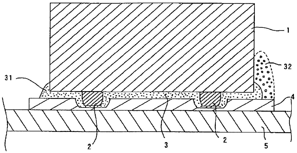
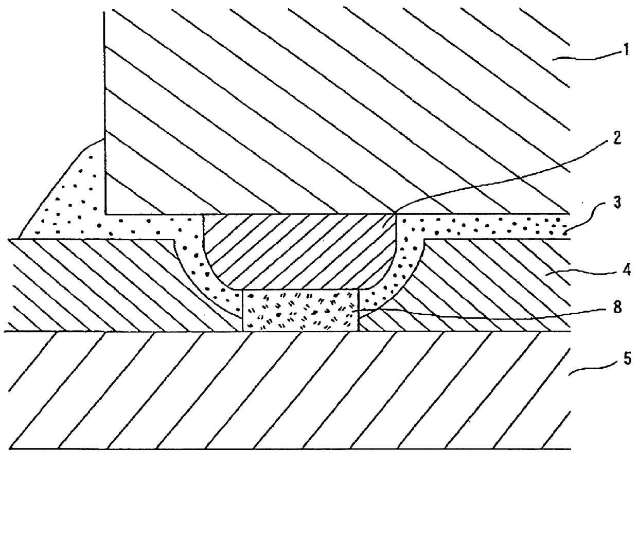
FIG. 1 shows an IC chip 1 having electrode pads formed on the surface of the IC chip 1. Bumps 2 are formed on the electrode pads of the IC chip 1 and are electrically and mechanically connected to a substrate 5 with paste-like adhesive 3 and an ACF 4.

More specifically, the IC chip 1 and the substrate 5 are heat-pressure bonded together with the paste-like adhesive 3 and the ACF 4 being placed between the IC chip 1 and the substrate 5, and the bumps 2 formed on the electrode pads of the IC chip 1 are electrically connected to a pattern formed on the substrate 5.

The paste-like adhesive 3 has a high fluidity, and can be coated on the surface of an object to be bonded. When a pressure force is applied to the IC chip 1 and the substrate 5 having the ACF 4 being placed therebetween, the coated paste-like adhesive 3 flows fr...


PUM


Abstract

An improved flip chip mounting method is provided for mounting an IC chip on a substrate. The IC chip has one surface and electrodes formed on the one surface, and the IC chip is positioned so that the electrodes oppose the substrate. The IC chip and the substrate are heat bonded to one another with a sheet of anisotropic conductive adhesive and paste-like adhesive being placed between the IC chip and the substrate.

Description

1. Field of the InventionThe present invention relates to a method of mounting an IC chip on a substrate and an apparatus manufactured by the method, and more particularly to a flip chip mounting method and a semiconductor apparatus formed thereby.2. Description of Related ArtIn a typical conventional flip chip mounting method, a sheet of anisotropic conductive adhesive or a film of anisotropic conductive adhesive (herein after referred to as ACF) 4 shown in FIG. 3, or anisotropic conductive adhesive paste-like (herein after referred to as ACP) 9 shown in FIG. 4 is placed between an IC chip 1 and a substrate 5. Then, the IC chip 1 and the substrate 5 are electrically and mechanically bonded to each other by heat pressure bonding.Also, as shown in FIG. 5, a molding material 6 is used to adhere an IC chip 1 to a substrate 5. The IC chip 1 has electrode pads formed on the surface of the IC chip and bumps 2 formed on the electrode pads, and the substrate 5 has a metal pattern formed on ...

Claims


Application Information

Patent Timeline
Patent Type & Authority Patents(United States)
IPC IPC(8): H01L21/56H01L21/02H01L21/60
CPCH01L21/563H01L24/29H01L24/81H01L2224/83851H01L2224/73203H01L2224/73204H01L2224/81801H01L2224/83191H01L2924/01004H01L2924/01078H01L2924/01079H01L2924/01082H01L2924/01322H01L2924/14H01L2924/01006H01L2924/01033H01L2924/014H01L2224/293H01L2224/2929H01L2224/29082H01L2224/29076H01L2224/2939H01L2224/83192H01L2224/81191H01L2224/81136H01L2224/16237H01L2924/07811H01L2224/32225H01L2224/16225H01L2224/73104H01L2924/3512H01L2924/00H01L2924/00012
Inventor SAKO, YUKITOSHI
Owner SEIKO EPSON CORP
Why Eureka
Try Eureka