Multilayered anisotropic conductive adhesive for fine pitch

a technology fine pitch, which is applied in the field of anisotropic conductive adhesive, can solve the problems of reducing electrical resistance, reducing electrical conductivity, and limited anisotropic conductive adhesives, and achieves the effects of reducing the cost of completing anisotropic conductive adhesives, increasing the adhesive strength between the substrate and the ic, and stable electrical conductivity

Inactive Publication Date: 2006-02-16
TELEPHUS
View PDF6 Cites 31 Cited by
  • Summary
  • Abstract
  • Description
  • Claims
  • Application Information

AI Technical Summary

Benefits of technology

[0019] Accordingly, in case where an IC is connected to a substrate, on which a plurality of electrodes are formed to a fine pitch, using an anisotropic conductive adhesive according to the present invention, the number of conductive particles in the anisotropic conductive adhesive flowing into the gaps between the bumps or the electrodes is reduced. Thus, the conductive particles can fully contribute to the electrical connection between the electrodes and the bumps, thereby obtaining stable electrical conductivity. Also, the adhesive strength between the substrate and the IC can be increased more and the costs for completing the anisotropic conductive adhesive can be reduced.

Problems solved by technology

However, a prior art anisotropic conductive adhesive is limited in connecting a drive IC to a substrate, on which electrodes are formed to a fine pitch.
In other words, when a drive IC is connected to a substrate, on which electrodes are formed to a fine pitch, using the prior art anisotropic conductive adhesive by the COG method or a chip-on-film (COF) method, a short-circuit may easily occur between adjacent bumps or adjacent electrodes due to a gap between the adjacent bumps or the adjacent electrodes.
However, if too many conductive particles are in the anisotropic conductive adhesive, the electrical resistance may be lowered and the possibility of short-circuits occurring becomes higher.
In contrast, if there are too few conductive particles, the number of conductive particles contributing to the electrical connection between electrodes is reduced, which may result in an increase in the resistance between the electrodes.
Thus, if the anisotropic conductive adhesive contains more than the proper number of conductive particles, a short-circuiting risk is increased, manufacturing costs are increased, and an excess of conductive particles exists in the gaps between the bumps or the electrodes.
As a result, the adhesive strength of the anisotropic conductive adhesive deteriorates.
However, in such a method, smooth adhesion cannot be achieved and voids are formed in the gaps, thereby deteriorating the mechanical strength of the anisotropic conductive adhesive as well as the adhesive strength.

Method used


Image

  • Multilayered anisotropic conductive adhesive for fine pitch
  • Multilayered anisotropic conductive adhesive for fine pitch
  • Multilayered anisotropic conductive adhesive for fine pitch

Examples


first embodiment

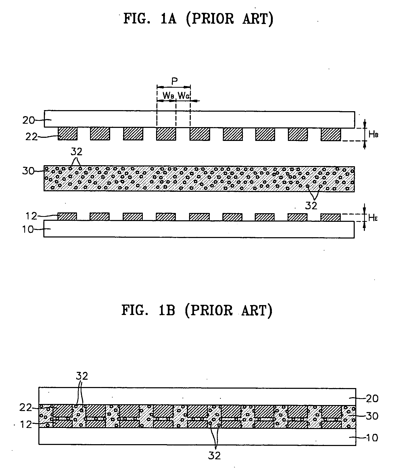
[0049]FIGS. 3A and 3B are a flowchart and a cross-sectional view explaining a method of manufacturing an anisotropic conductive adhesive 140 according to the present invention. In FIGS. 3A and 3B, a method of manufacturing the anisotropic conductive adhesive 140 which can be used to connect an IC 130, on which a plurality of bumps 132 are formed, to a glass substrate 120, on which a plurality of ITO electrodes 122 are formed to a fine pitch, by a COG method will be described. In general, the ITO electrodes 122 on the glass substrate 120 each have a height of about 2 μm, which is less than the average particle diameter (in general about 3-5 μm) of conductive particles 143. Thus, in this embodiment, a method of manufacturing the anisotropic conductive adhesive 140 of a two-layered structure, which has one surface facing the IC 130 on which a nonconductive adhesive layer is formed and the other surface facing the glass substrate 120 on which a nonconductive adhesive layer is not formed...

second embodiment

[0057]FIGS. 4A and 4B are respectively a flowchart and a cross-sectional view explaining a method of manufacturing an anisotropic conductive adhesive 240 according to the present invention. In FIGS. 4A and 4B, a method of manufacturing the anisotropic conductive adhesive 240 which can be used to connect an IC 230, on which bumps 232 are formed, to a substrate 220, which is made of a flexible film, e.g., a polyimide film, and on which a plurality of metal electrodes 222 made of Cu or Al are formed to a fine pitch, by a COF method will be described. In general, the metal electrodes 222 on the substrate 220 made of the flexible film each have a height HE2 of no greater than about 15 μm more than the height of the ITO electrodes formed on a glass substrate. Thus, in this embodiment, there will be described a method of manufacturing the anisotropic conductive adhesive 240 of a triple-layered structure which has one surface facing the IC 230 on which a nonconductive adhesive layer is form...

fourth embodiment

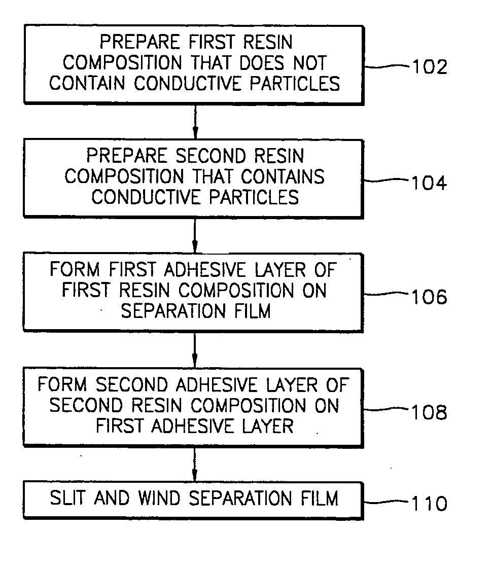
[0072]FIGS. 6A through 6C are a flowchart and cross-sectional views explaining a method of manufacturing an anisotropic conductive adhesive 440 according to the present invention. In this embodiment, a method of manufacturing the anisotropic conductive adhesive 440 which can be used to connect an IC 430, on which bumps 432 are formed, to a substrate 420, which is made of a flexible film, e.g., a polyimide film, and on which a plurality of metal electrodes 422 made of Cu or Al are formed to a fine pitch, by the COF method will be described. In this embodiment, described will be a method of manufacturing the anisotropic conductive adhesive 440 of a triple-layered structure which has one surface facing the IC 430 on which a nonconductive adhesive layer is formed and the other surface facing the substrate 420 made of the flexible film on which a nonconductive adhesive layer is formed.

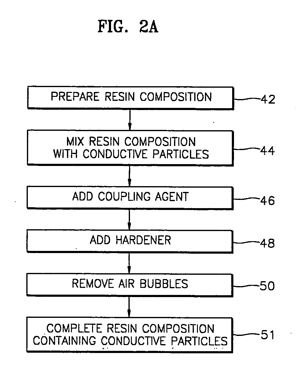
[0073] Referring to FIGS. 6A through 6C, in steps 402 and 404, a nonconductive first resin composition t...


PUM


Abstract

Provided is an anisotropic conductive adhesive for a fine pitch having a conductive adhesive layer and a nonconductive adhesive layer formed on one surface or both surfaces of the conductive adhesive layer. The anisotropic conductive adhesive for a fine pitch can be used to adhere an integrated circuit, on which a plurality of bumps each having a second height are formed, to a substrate, on which a plurality of electrodes each having a first height are formed keeping predetermined distances from each other, so that the integrated circuit is electrically connected to the electrodes. The anisotropic conductive adhesive includes a nonconductive first adhesive layer and a second adhesive layer. The nonconductive first adhesive layer includes a thermosetting resin and a hardener for hardening the thermosetting resin and has a first thickness of ½- 3/2 of the second height. The second adhesive layer includes a thermosetting resin, a hardener for hardening the thermosetting resin, and a plurality of conductive particles each having an average particle diameter of ½ or less of the width of gaps between the plurality of electrodes and a first density dispersion, has a second thickness larger than two times the average particle diameter of the conductive particles, and is formed on one surface of the nonconductive first adhesive layer.

Description

BACKGROUND OF THE INVENTION [0001] 1. Field of the Invention [0002] The present invention relates to an anisotropic conductive adhesive, and more particularly, to an anisotropic conductive adhesive which is used to connect a drive integrated circuit (IC) to a substrate on which electrodes are formed to a fine pitch. [0003] 2. Description of the Related Art [0004] Methods of mounting a drive IC on a liquid crystal display (LCD) panel can be classified into a wire-bonding method, a tape automated bonding (TAB) method, a chip-on-glass (COG) method, and the like. In the wire-bonding method, a drive IC is bonded to electrodes on a LCD panel via conductive wires. In the TAB method, a drive IC is mounted on electrodes on a LCD panel using a base film. In the COG method, a drive IC is mounted directly on a LCD panel using a predetermined adhesive. Among theses methods, the COG method has advantages in that an area for mounting a drive IC over a LCD panel can be minimized and the costs for m...

Claims


Application Information

Patent Timeline
Patent Type & Authority Applications(United States)
IPC IPC(8): H01L23/48
CPCH01L24/29H01L24/83H01L2224/16225H01L2224/73204H01L2224/83101H01L2924/01002H01L2924/01013H01L2924/01015H01L2924/01029H01L2924/0103H01L2924/01049H01L2924/0105H01L2924/01078H01L2924/01079H01L2924/0781H01L2924/14H05K3/323H05K2201/0209H05K2201/0212H05K2203/1189H01L2224/29H01L2224/2919H01L2924/01006H01L2924/01033H01L2924/0665H01L2224/29455H01L2224/2929H01L2224/293H01L2224/29386H01L2224/29388H01L2224/29444H01L2924/00013H01L2924/07811H01L2924/07802H01L2224/29082H01L2224/29083H01L2224/83851Y10T428/1059H01L2924/00014H01L2924/05442H01L2924/05432H01L2924/04642H01L2924/00H01L2224/29099H01L2224/29199H01L2224/29299C09K2323/05H01L2924/00011H01L2224/0401
Inventor YIM, MYUNG JINHWANG, JIN SANG
Owner TELEPHUS
Why Eureka
Try Eureka