Method of manufacturing light-emitting diode

a technology of light-emitting diodes and manufacturing methods, which is applied in the direction of semiconductor devices, lighting and heating apparatus, light sources, etc., can solve the problems of low manufacturing efficiency, unfavorable automatic manufacturing, and generally involves a relatively high manufacturing cos

Inactive Publication Date: 2010-10-12
HON HAI PRECISION IND CO LTD
View PDF1 Cites 31 Cited by
  • Summary
  • Abstract
  • Description
  • Claims
  • Application Information

AI Technical Summary

Problems solved by technology

However, such method has a low manufacturing efficiency and is unfavorable to realize automatic manufacturing.
Therefore, such method generally involves a relatively high manufacturing cost.

Method used


Image

  • Method of manufacturing light-emitting diode
  • Method of manufacturing light-emitting diode
  • Method of manufacturing light-emitting diode

Examples


Embodiment Construction

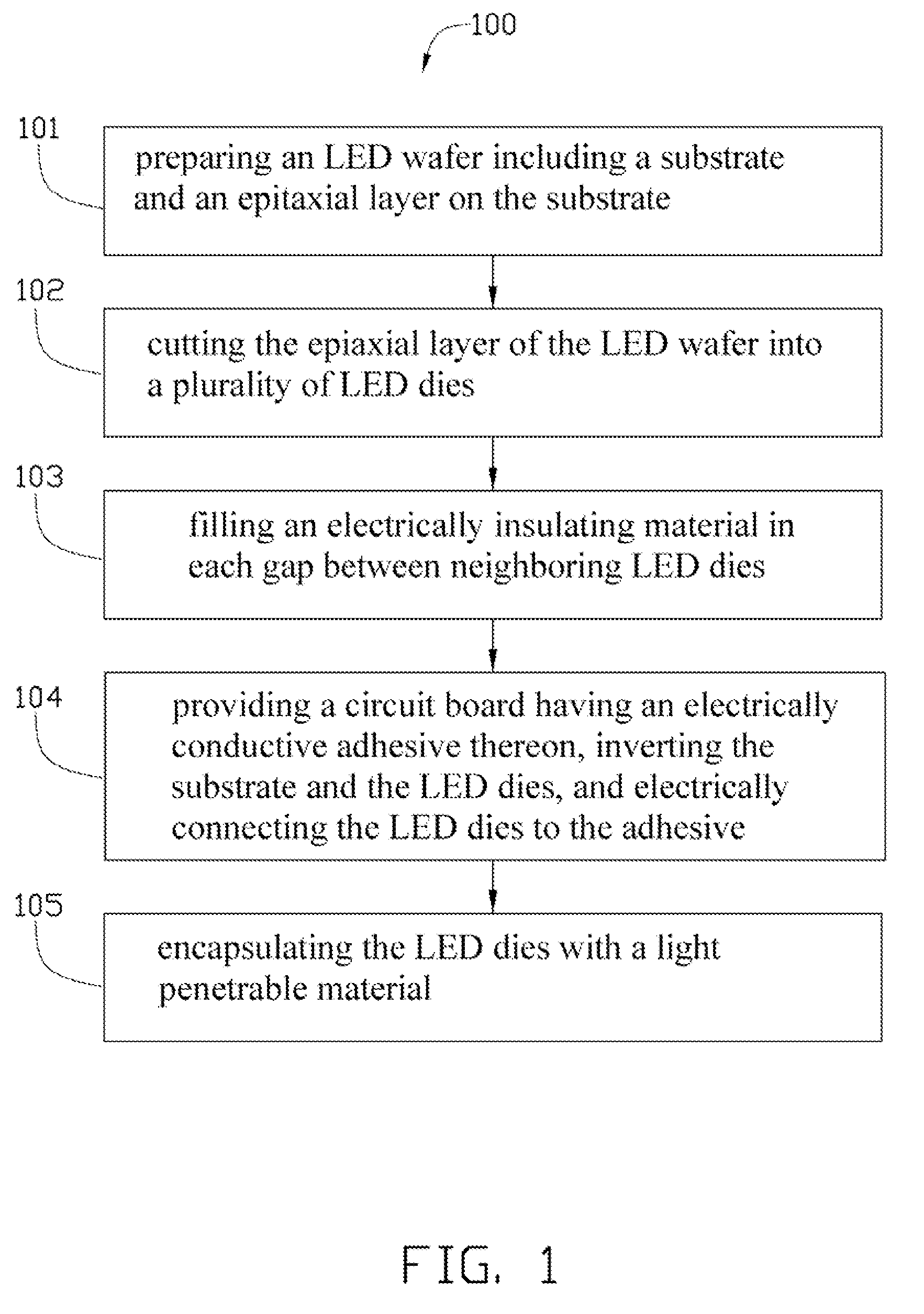
[0016]FIG. 1 shows a method 100 of manufacturing an LED in accordance with an embodiment of the present disclosure. The method includes steps 101, 102, 103, 104, 105, which will be disclosed in detail herebelow.

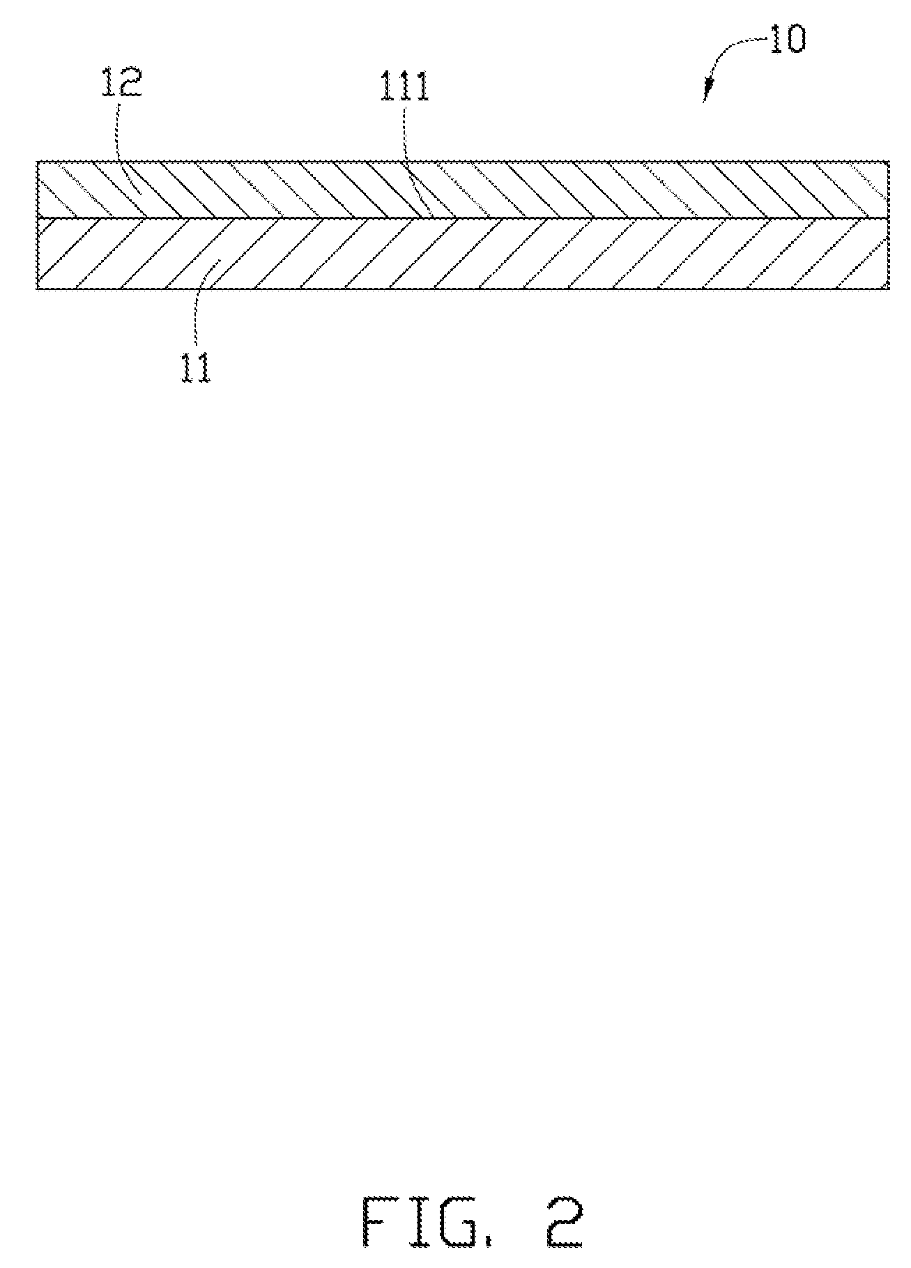
[0017]Referring to FIG. 1 and FIG. 2, in the step 101, an LED wafer 10 is prepared, wherein the LED wafer 10 includes a substrate 11 and an epitaxial layer 12 formed on the substrate 11. The substrate 11 may be a sapphire substrate. The epitaxial layer 12 is formed on a top surface 111 of the substrate 11. The epitaxial layer 12 forms as a p-n junction type semiconductor light-emitting structure. The p-n junction type semiconductor light-emitting structure may be gallium nitride-based III-V group compound semiconductor.

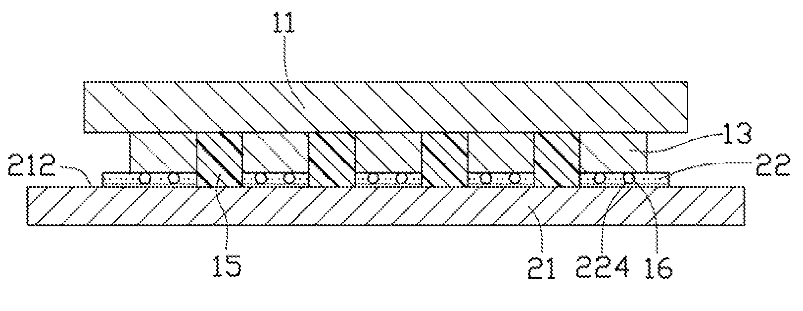
[0018]Referring to FIG. 1 and FIG. 3, in the step 102, the epitaxial layer 12 of the LED wafer 10 is cut into a plurality of LED dies 13. The LED dies 13 are arranged in rows and columns on the substrate 11. The LED dies 13 are separated from each other with a ...


PUM


Abstract

A method of manufacturing an LED includes the following steps: preparing an LED wafer including a substrate and an epitaxial layer formed on the substrate; cutting the epitaxial layer of the LED wafer into a plurality of LED dies with a gap defined between every two neighboring dies; filling an electrically insulating material in each gap between neighboring LED dies such that the neighboring LED dies are separated from each other by the insulating material; providing a circuit board having a layer of anisotropic conductive adhesive coated thereon; pressing the LED dies against the adhesive to bring the top surfaces of the LED dies into contact with the adhesive such that the LED dies each are electrically connected to the circuit board via the adhesive; and encapsulating the LED dies with a light penetrable material.

Description

BACKGROUND[0001]1. Technical Field[0002]The present disclosure relates to LEDs (light emitting diodes), and particularly to a method of manufacturing an LED.[0003]2. Description of Related Art[0004]Presently, LEDs are preferred for use in non-emissive display devices than CCFLs (cold cathode fluorescent lamp) due to their high brightness, long lifespan, and wide color range.[0005]In manufacturing an LED, most of the methods involve the following steps. Firstly, an LED wafer is provided and the LED wafer is cut into a plurality of individual LED dies. The LED dies are then disposed on a circuit board one by one, and each of the LED dies is independently encapsulated to form an LED. However, such method has a low manufacturing efficiency and is unfavorable to realize automatic manufacturing. Therefore, such method generally involves a relatively high manufacturing cost.[0006]Therefore, a new method of manufacturing an LED is desired to overcome the above described shortcoming.BRIEF DE...

Claims


Application Information

Patent Timeline
Patent Type & Authority Patents(United States)
IPC IPC(8): H01L21/00
CPCH01L25/0753F21K9/00H01L24/81H01L2224/73204H01L2224/95H01L2924/0002H01L2924/12041H01L2924/00
Inventor LAI, CHIH-CHEN
Owner HON HAI PRECISION IND CO LTD
Why Eureka
Try Eureka