Semiconductor apparatus and method for producing same

Inactive Publication Date: 2001-09-25
CANON KK
View PDF14 Cites 33 Cited by
  • Summary
  • Abstract
  • Description
  • Claims
  • Application Information

AI Technical Summary

Problems solved by technology

With these panel increasing tendency and pixel micronization tendency, decrease is encountered in the yield in TFT panel production steps.
(1) a wiring distance per panel has been increasing with progress in the size increasing tendency of the panel, and a discontinuity probability becomes higher therewith;
(2) the area of TFTs and wiring cross portions per panel has been increasing with progress in the micronization tendency of the pixel pattern of panel, and a short probability thus becomes higher between upper and lower metal wires;
(3) electrostatic damage (ESD); specifically, the area capable of contacting the outside has been increasing with the size increasing tendency of panel, so as to increase the quantity of sta

Method used


Image

  • Semiconductor apparatus and method for producing same
  • Semiconductor apparatus and method for producing same
  • Semiconductor apparatus and method for producing same

Examples


embodiment 1

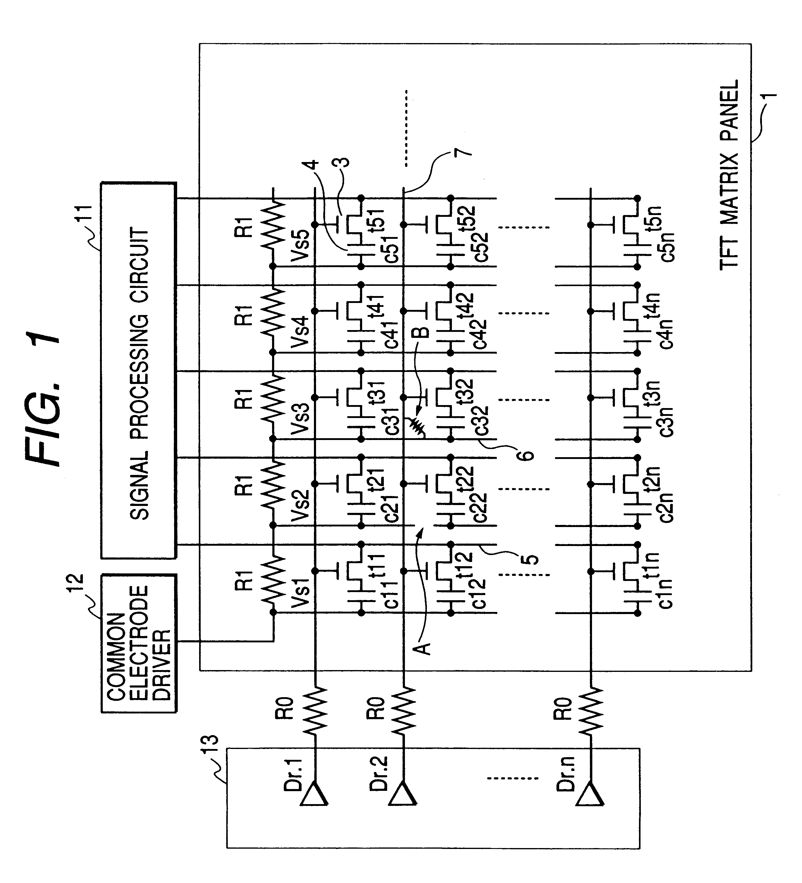
FIG. 3 is an equivalent circuit diagram of a TFT matrix panel in Embodiment 1 of the present invention. The present embodiment is an example of application of the TFT panel to the photoelectric conversion apparatus.

In FIG. 3 like symbols denote the same or similar members as those in FIG. 1 and the description thereof is omitted herein. In the present embodiment numeral 4 denotes the photoelectric conversion elements. The photoelectric conversion elements suitably applicable are the photodiode type or the MIS type (for example, having the stacked structure composed at least of an electrode, an insulating layer, a semiconductor layer for photoelectric conversion, and an ohmic contact layer (n.sup.+ type semiconductor layer) on a substrate) photosensors.

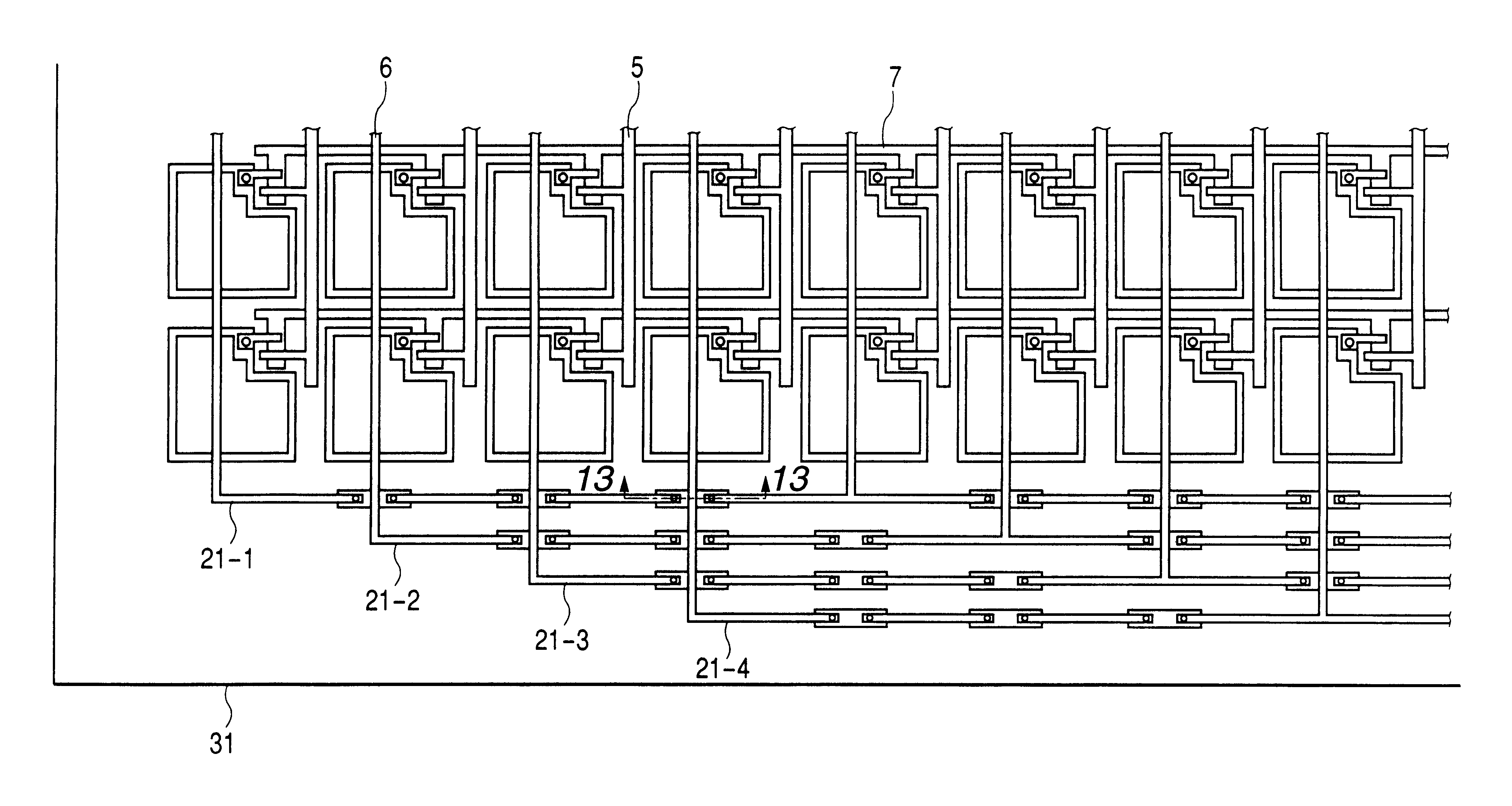
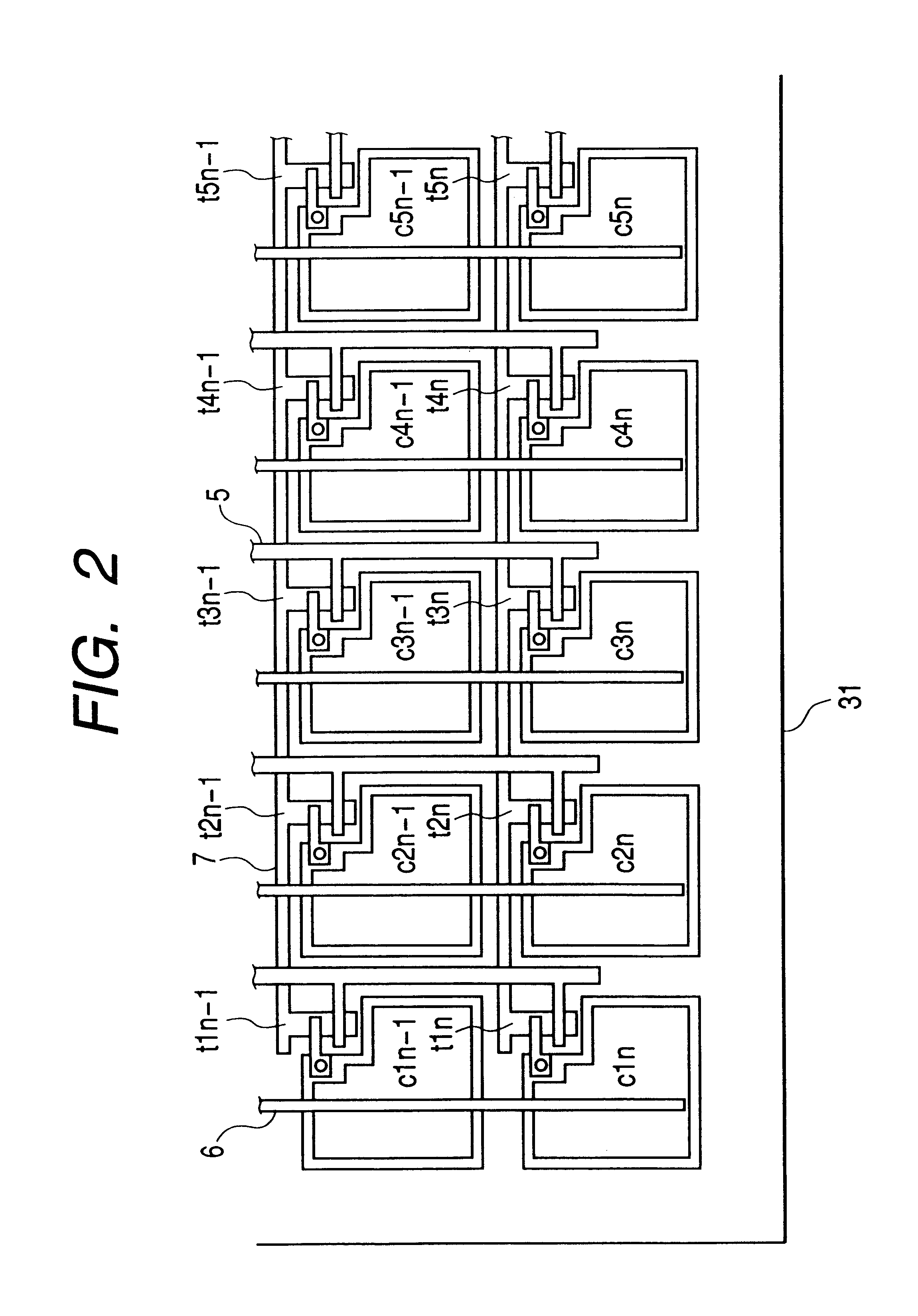
In FIG. 3 a redundant wire 21 is provided so as to be common to the bias lines.

FIG. 4 is a schematic pattern diagram at a corner part on the opposite side to the bias application side to the bias lines 6 by the common electrode driver ...

embodiment 2

FIG. 6 is a schematic equivalent circuit diagram of a TFT matrix panel according to Embodiment 2 of the present invention. The present embodiment is an example of application of the TFT panel to the photoelectric conversion apparatus.

In FIG. 6 reference is made to the description of FIG. 1 as to the same members as those in FIG. 1 and the description thereof is omitted herein.

first embodiment

The present embodiment is identical to the first embodiment in that the second electrodes of the photoelectric conversion elements (c11 to cmn) are connected to the plurality of bias lines 6 connected to the common electrode driver 12, but the present embodiment is different therefrom in that the bias lines 6 are grouped into two series and the bias voltage can be applied to the bias lines 6 in each series from either one of two common electrode drivers 12.

The present embodiment will be described under the assumption that the photoelectric conversion elements are the MIS type sensors. After transfer of signals, electrons stored in the second electrodes of the photoelectric conversion elements (in which capacitors are established) c11 to cmn are eliminated by applying the bias from the common electrode drivers 12 to the n.sup.+ type semiconductor layer (forming one electrode).

FIG. 7 is a schematic pattern diagram at a corner part on the opposite side to the bias application side to t...


PUM


Abstract

In order to prevent a decrease of yield due to a discontinuity of a wire or a short between upper and lower metal wires in production of a TFT matrix panel having pixel capacitors and TFTs and produce the TFT panel in a good yield without decrease of an aperture rate of the pixel capacitor portions even with increase in the size of the panel and with micronization of the pixel pattern, ends of bias lines on the opposite side to connection to a common electrode driver for application of bias are electrically connected to each other by a redundant wire.

Description

1. Field of the InventionThe present invention relates to a semiconductor apparatus and a method for producing it and, more particularly, to a semiconductor apparatus having a thin film transistor (TFT) matrix panel, which is suitably applicable, for example, to formation of a liquid crystal display apparatus or a photoelectric conversion apparatus, and a method for producing it.2. Related Background ArtIt has been a widespread practice heretofore to construct a display unit of a display device such as a liquid crystal panel or the like or a reading unit of a photoelectric conversion device such as an area sensor of a lot of display pixels or reading pixels arrayed in an X-Y matrix and to carry out signal input to each pixel or signal reading from each pixel by an X-Y matrix driving method via TFT provided for each pixel. The display pixels of the display device can be constituted using a liquid-crystal display element in which the liquid crystal is interposed between a pair of elec...

Claims


Application Information

Patent Timeline
IPC IPC(8): G02F1/13G02F1/1362G09G3/36G02F1/1343G02F1/136G02F1/1368G09F9/00G09F9/30H01L29/786H04N5/335H04N5/369H04N5/374
CPCG02F1/136204H04N5/32G02F1/136259G09G2330/08G09G3/3648
Inventor WATANABE, MINORUMOCHIZUKI, CHIORIISHII, TAKAMASA
Owner CANON KK
Why Eureka
Try Eureka