Optimal design of an inductor and inductor circuit

a technology of inductors and circuits, applied in the direction of cad circuit design, program control, instruments, etc., can solve the problems of insufficient optimization tools for circuit design, inability to use a library of previously fabricated inductors or generating, and inability to optimize circuits

Inactive Publication Date: 2001-10-30
THE BOARD OF TRUSTEES OF THE LELAND STANFORD JUNIOR UNIV
View PDF5 Cites 39 Cited by
  • Summary
  • Abstract
  • Description
  • Claims
  • Application Information

AI Technical Summary

Problems solved by technology

The parasitic resistance and capacitance associated with these spiral inductors result in several engineering trade-offs.
Unfortunately, no inductor optimization tool exists to aid in circuit design.
Currently most designers are limited to use of a library of previously fabricated inductors or generating a large database of inductors using a 3-D field solver.
While the former option severely constrains the ava

Method used


Image

  • Optimal design of an inductor and inductor circuit
  • Optimal design of an inductor and inductor circuit
  • Optimal design of an inductor and inductor circuit

Examples


Embodiment Construction

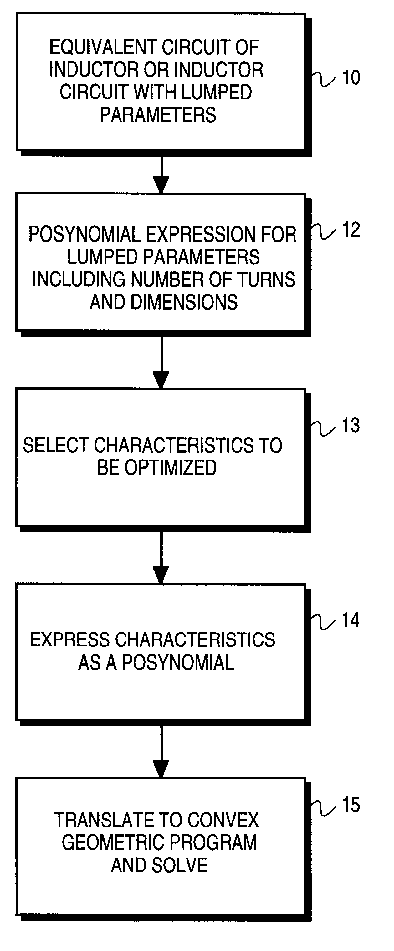
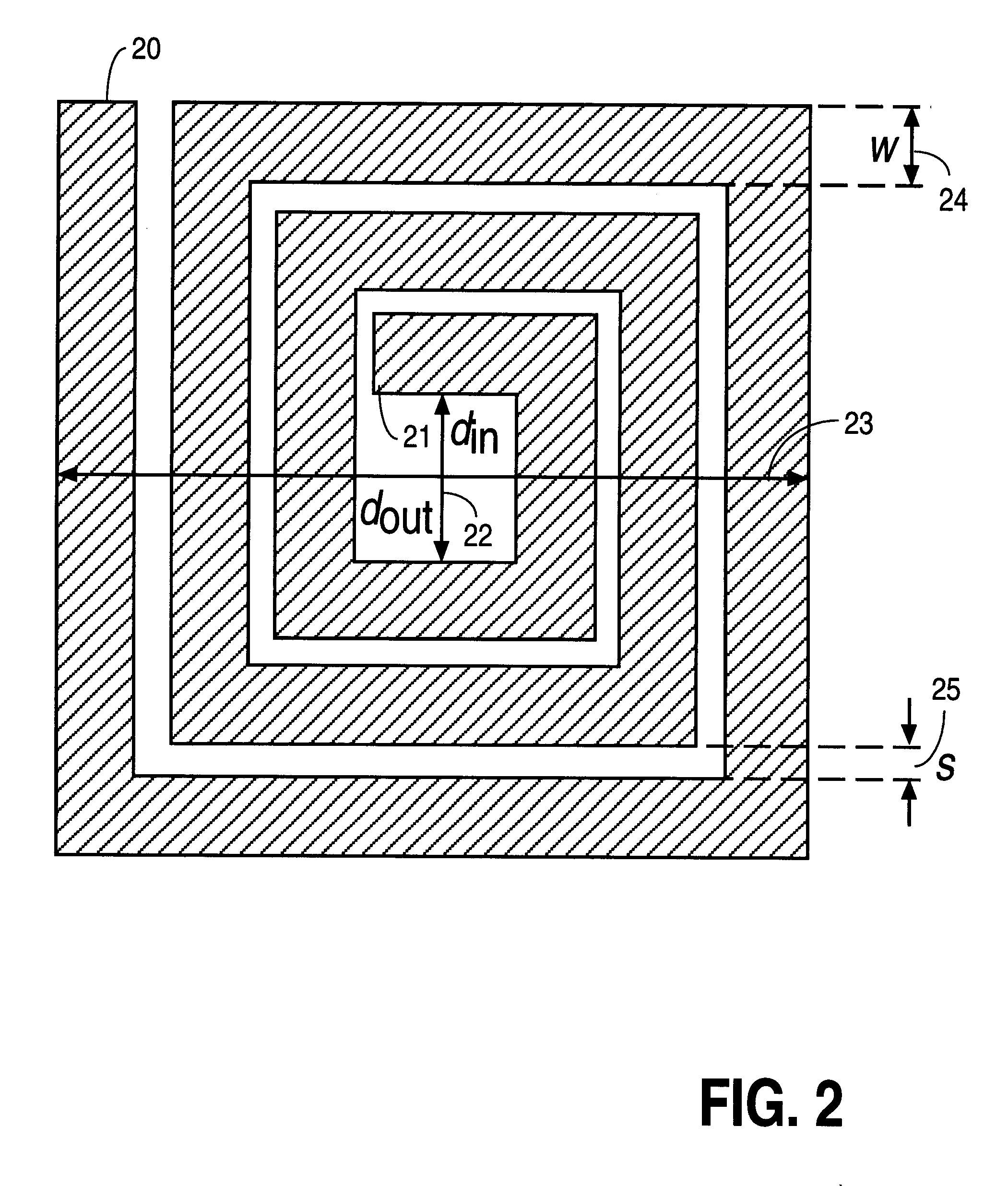
A method is described for optimizing inductors and inductor circuits and more particularly useful in integrated circuits to optimize RF inductors and inductor circuits. In the following description numerous specific details will be set forth in order to provide a thorough understanding of the present invention. It will be apparent to one skilled in the art that the present invention may be practiced without these specific details. In other instances, well-known mathematical techniques have not been described in detail in order not to obscure the present invention.

In co-pending application patent application Ser. No. 09 / 123,129, filed Jul. 28, 1998, entitled "System and Method for Designing Integrated Circuits," computer aided design tools for designing globally optimal integrated circuits using geometric programs is described. As described in automated synthesis of globally optimal circuit designs for a given circuit topology library is obtained directly from a user defined specific...


PUM


Abstract

A method for the design and optimization of inductors for RF circuits. This method consists in the formulation of RF circuit designs as geometric programs. The designer can specify a wide variety of specifications such as gain, bandwidth, noise, etc. The method, which was implemented in simple code, determines inductor dimensions and component values in a few seconds real-time. The results was also a globally optimal design.

Description

BACKGROUND OF THE DISCLOSURE1. Field of the InventionThe invention relates to the field of designing inductors and inductor circuits particularly for integrated circuits.2. Prior ArtThere is a growing need for optimally designed inductors and integrated circuit, as radio-frequency integrated circuits (RFICs) become more widely used in low-cost communications. This, for instance, has created great demand and interest in on-chips spiral inductors. The parasitic resistance and capacitance associated with these spiral inductors result in several engineering trade-offs. Unfortunately, no inductor optimization tool exists to aid in circuit design. Currently most designers are limited to use of a library of previously fabricated inductors or generating a large database of inductors using a 3-D field solver. While the former option severely constrains the available design space, the latter one requires a sophisticated search engine and is numerically expensive, especially when process param...

Claims


Application Information

Patent Timeline
IPC IPC(8): G06F17/50
CPCG06F17/5063G06F30/36
Inventor HERSHENSON, MARIA DEL MARBOYD, STEPHEN P.MOHAN, SUNDERARAJAN S.
Owner THE BOARD OF TRUSTEES OF THE LELAND STANFORD JUNIOR UNIV
Why Eureka
Try Eureka