Apparatus for and method of automatic optical inspection of electronic circuit boards, wafers and the like for defects, using skeletal reference inspection and separately programmable alignment tolerance and detection parameters

an automatic optical inspection and electronic circuit board technology, applied in the field of automatic optical inspection of electronic circuit boards, wafers and the like, can solve the problems of reducing the accuracy of commercial mechanical stage systems, unable to provide such accuracy, and unable to reach the level of precision

Inactive Publication Date: 2002-07-30
BELTRONICS
View PDF7 Cites 31 Cited by
  • Summary
  • Abstract
  • Description
  • Claims
  • Application Information

AI Technical Summary

Benefits of technology

An object of the present invention, accordingly, is to provide a new and improved method of and apparatus for automatically optically inspecting for defects, electronic parts, such as wafers, chips, circuit boards and the like

Problems solved by technology

To avoid missing all defects in the sample, however, requires very precise alignment of the sample and reference images, which demands perfect overlap.
Commercial mechanical stage systems simplify cannot provide such accuracy; and even to approach that level

Method used


Image

  • Apparatus for and method of automatic optical inspection of electronic circuit boards, wafers and the like for defects, using skeletal reference inspection and separately programmable alignment tolerance and detection parameters
  • Apparatus for and method of automatic optical inspection of electronic circuit boards, wafers and the like for defects, using skeletal reference inspection and separately programmable alignment tolerance and detection parameters
  • Apparatus for and method of automatic optical inspection of electronic circuit boards, wafers and the like for defects, using skeletal reference inspection and separately programmable alignment tolerance and detection parameters

Examples


Embodiment Construction

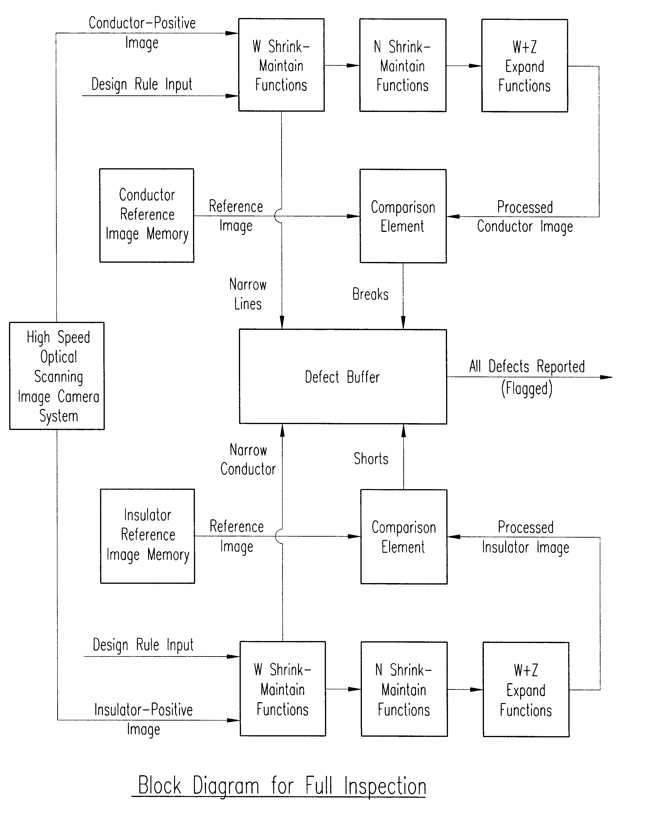
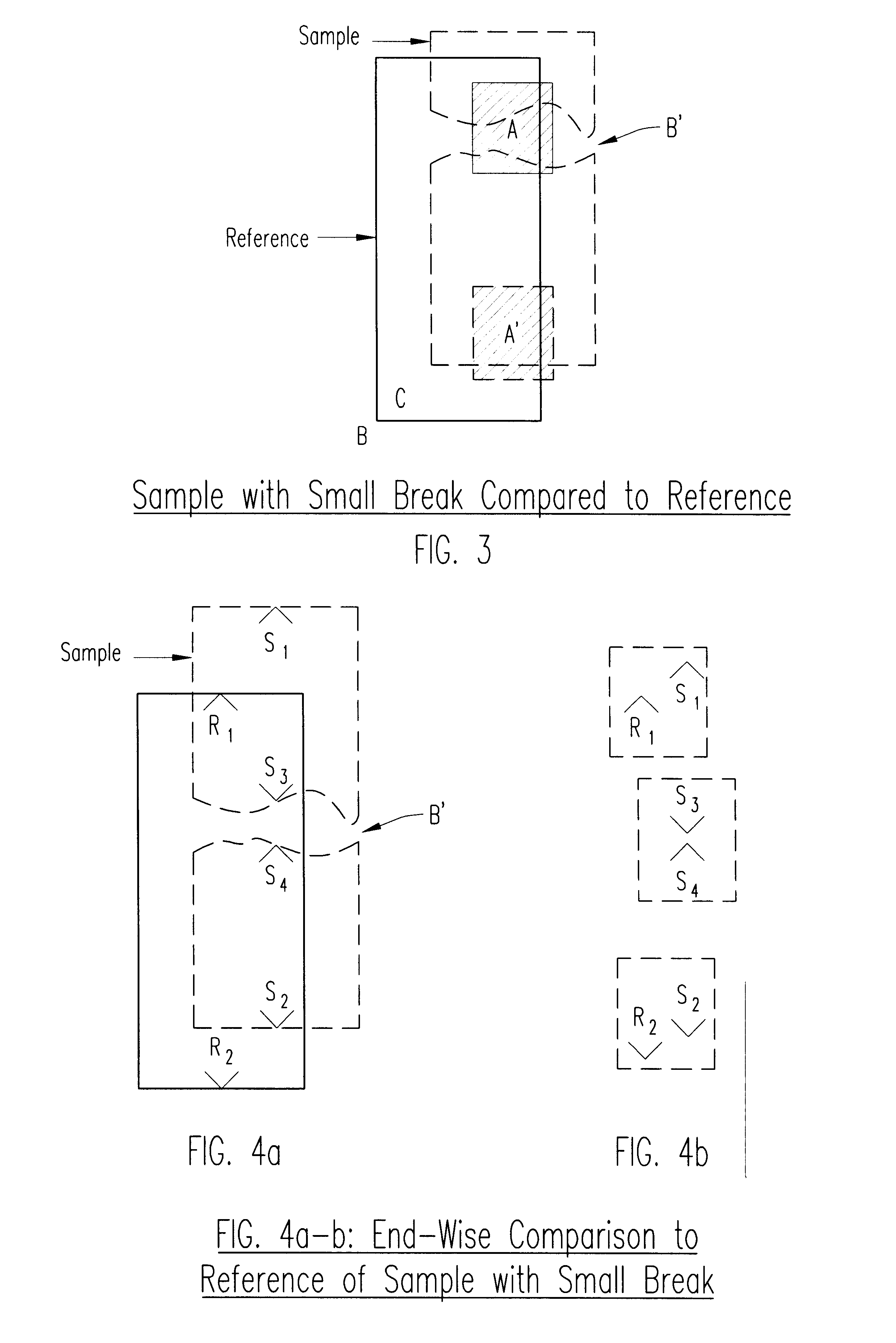
Before proceeding to describe preferred forms of the apparatus and method underlying the invention, and further to contrast the invention from pattern recognition and comparison systems of the prior art, earlier described, it is believed useful to illustrate the previously explained defect inspection limitations of such prior approaches.

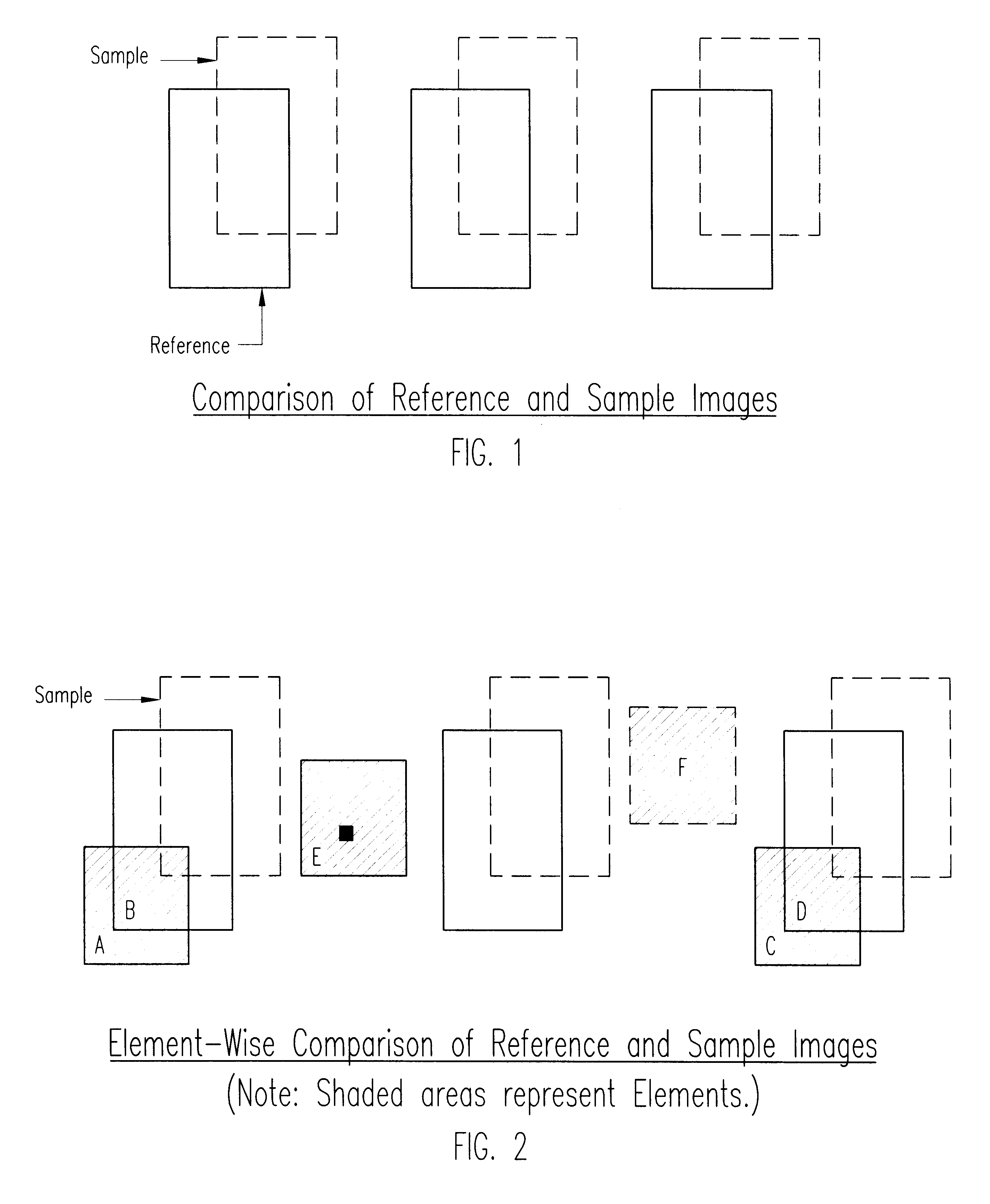
First, in connection with the before-mentioned prior comparison of the inspected sample part to the reference image, reference is made to FIG. 1, illustrating that the first obvious problem encountered is one of basic alignment. The solid line shows the stored reference image, while the dotted line shows the inspection image. Since, as shown, the reference image matches exactly the sample image, the two must overlap perfectly for a successful inspection--a task not easily accomplished. Historically, the optical image of a part of a sample-to-be-inspected, or a computer cad generated image of the part, is loaded into a computer or reference memory and...


PUM


Abstract

A novel wafer or circuit board automatic scanning optical inspection system and technique using the reference comparison principle for finding defects in scanned sample images, that enables a new degree of universality in finding all defects including very small single pixel conductor breaks and shorts and defects of irregular shapes, and together with simultaneous design rule processing, through the use of processed skeletal reference images and with separately programmable alignment tolerance and detection parameters.

Description

The present invention relates to automatic optical inspection apparatus and techniques for scanning surfaces to detect defects in manufacture, particularly though not exclusively useful for the inspection of multi-layer semiconductor devices and the like, such as wafers, chips, circuit boards, etc., wherein metal conductor patterns are provided on non-metal or insulative surfaces. Current methods using reference comparison inspection have specific shortcomings that cause them to miss certain identifiable classes of defects. The new method of reference comparison of the present invention is directed to avoiding these shortcomings and therefore now enabling the reliable finding of all defects.One method of prior reference inspection stores a correct image of the part and compares each inspected sample part to this reference image. To avoid missing all defects in the sample, however, requires very precise alignment of the sample and reference images, which demands perfect overlap. Comm...

Claims


Application Information

Patent Timeline
IPC IPC(8): G01R31/28G01R31/311G06T7/00
CPCG01R31/311G06T7/001G06T2207/30148
Inventor BISHOP, ROBERT
Owner BELTRONICS
Why Eureka
Try Eureka