Combinational test pattern generation method and apparatus

a test pattern and pattern technology, applied in the field of integrated circuit testing, can solve the problems of reducing the size of the region manipulated virtually every week, the design process rarely proceeds at a lower level, and the region affected by the selective manipulation of a single piece of semiconductor material is almost unimaginably small

Inactive Publication Date: 2002-11-12
RENESAS ELECTRONICS AMERICA
View PDF7 Cites 84 Cited by
  • Summary
  • Abstract
  • Description
  • Claims
  • Application Information

AI Technical Summary

Problems solved by technology

However, as noted, the design process rarely proceeds at a lower level than that of logic diagrams.
The regions affected by the selective manipulation of the single piece of semiconductor material are almost unimaginably small.
Furthermore, the sizes of the regions manipulated decrease virtually every week.
Due to the very small regions manipulated during VLSI production, errors invariably occur.
This can be the result of contamination of the material, or minor variations in the length, width, or height of lines etched.
These errors in production often result in errors in the behavior of the discrete electronic circuit level components.
Consequently, errors in production sufficient to produce errors in the behavior of the discrete circuit level components can "propagate" upwards to the logic diagram level since the logic diagram circuits are built from congeries of these malfunctioning circuit components.
If the errors are severe, then such malfunctioning will be very apparent in that the affected logic diagram level circuits will not function.
However, if the malfunction is not severe, it is possible that the affected logic diagram level components will perform, but will perform in such a way that is out of design tolerances, which can cause a general system malfunction or failure as these logic diagram level errors "propagate" up the abstraction-layer hierarchy to affect the RTL and functional block diagram level designs.
Those skilled in the art will recognize that, due to the foregoing noted difficulties, it is the practice within the related art to design scan chain test pattern sets dependent upon the inputs of any particular circuit under test, which thus severely limits the number of test pattern sets which can be utilized.
However, it has been demonstrated that under the related art it is not possible to practicably apply the full range of test pattern sets appropriate to a particular combinational logic circuit under test.

Method used


Image

  • Combinational test pattern generation method and apparatus
  • Combinational test pattern generation method and apparatus
  • Combinational test pattern generation method and apparatus

Examples


Embodiment Construction

)

The following sets forth a detailed description of the best contemplated mode for carrying out the invention as described in the claims. The detailed description is intended to be illustrative and should not be taken as limiting.

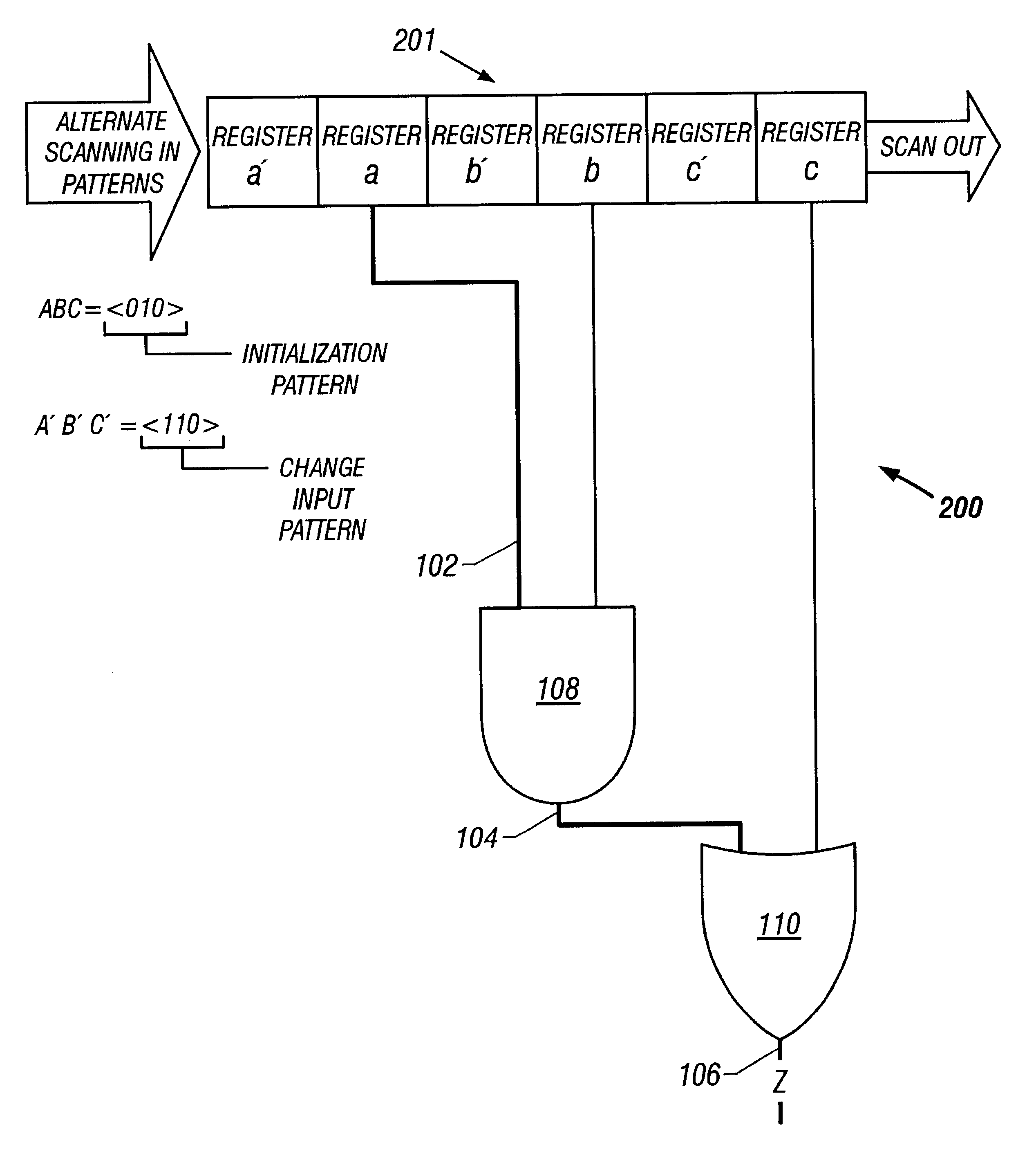
Referring now to FIGS. 2A, 2B, and 2C shown is a combinational logic circuit 200 composed of logic diagram level circuits which will be utilized to illustrate the functioning of embodiments of the present invention. Depicted in FIG. 2A is that shadowed scan chain register bank 201 is feeding combinational logic circuit 200. As shown, shadowed scan chain register bank 201 has Registers a, b, and c of scan chain register bank 101; however, also shown is that shadowed scan chain register bank 201 has "shadow" Register b' inserted between Registers a and b, shadow Register c' inserted between Registers b and c, and shadow Register a' inserted to be the input register, and thus is shown inserted to the left of Register a.

As will be shown in the discussions of FI...


PUM

PropertyMeasurementUnit
lengthaaaaaaaaaa
semi-conductingaaaaaaaaaa
conductingaaaaaaaaaa

Abstract

A method and apparatus that couple a change input scan chain test pattern with an initialization scan chain test pattern such that a resultant scan chain test pattern is produced, and apply the resultant scan chain test pattern to at least one combinational logic path. In one embodiment, the coupling is achieved by interleaving the change input scan chain test pattern with the initialization scan chain test pattern. In another embodiment, the coupling is achieved by creating a constructed test pattern set from the change input and the initialization scan chain test pattern.

Description

1. Field of the InventionThis invention relates to the field of integrated circuit testing.2. Description of the Related ArtAn integrated circuit (IC) is a miniature electric circuit containing large numbers of discrete electronic circuit elements, such as transistors, resistors, capacitors, and diodes, which are packaged as a single unit with leads extending from it for input, output, and power-supply connections. The electronic circuit elements are formed by selective manipulation of a single chip of semiconductor material, often in combination with various other semi-conducting and / or conducting materials.It is common in the art to roughly classify integrated circuits dependent upon their transistor density. Presently, there are effectively four common integrated circuit classifications: small-scale integrated circuits (SSIs); medium-scale integrated circuits (MSIs); large-scale integrated circuits (LSIs); and very-large-scale integrated circuit (VLSIs). Exactly what transistor d...

Claims


Application Information

Patent Timeline
Patent Type & Authority Patents(United States)
IPC IPC(8): G01R31/3183G01R31/28G11B20/18
CPCG01R31/318371G11B20/1816
Inventor KOE, WERN-YAN
Owner RENESAS ELECTRONICS AMERICA
Why Eureka
Try Eureka