Apparatus and method for enhanced degassing of semiconductor wafers for increased throughput

a technology of enhanced degassing and semiconductor wafers, applied in electrical apparatus, conveyor parts, semiconductor devices, etc., can solve problems such as inability to meet the requirements of uniform wafer heating, degassing defects in integrated circuits,

Inactive Publication Date: 2002-12-24
NOVELLUS SYSTEMS
View PDF14 Cites 303 Cited by
  • Summary
  • Abstract
  • Description
  • Claims
  • Application Information

AI Technical Summary

Benefits of technology

is to provide an apparatus and process for degas of semiconductor wafers utiliz...

Problems solved by technology

If left to reside on and within the wafer, these impurities may result in defects in the integrated circuit.
However, the inherent design of these systems requires the wafers to be processed and heated in batch.
However, these designs promote batch processing, which requires a station...

Method used


Image

  • Apparatus and method for enhanced degassing of semiconductor wafers for increased throughput
  • Apparatus and method for enhanced degassing of semiconductor wafers for increased throughput
  • Apparatus and method for enhanced degassing of semiconductor wafers for increased throughput

Examples


Embodiment Construction

)

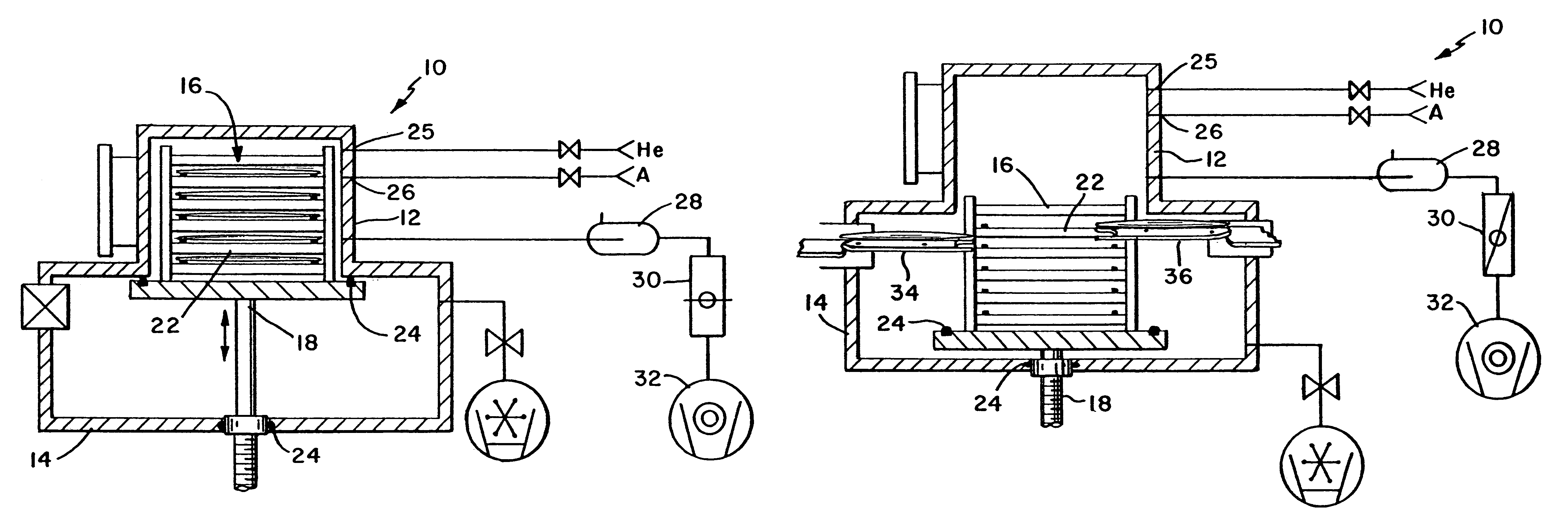
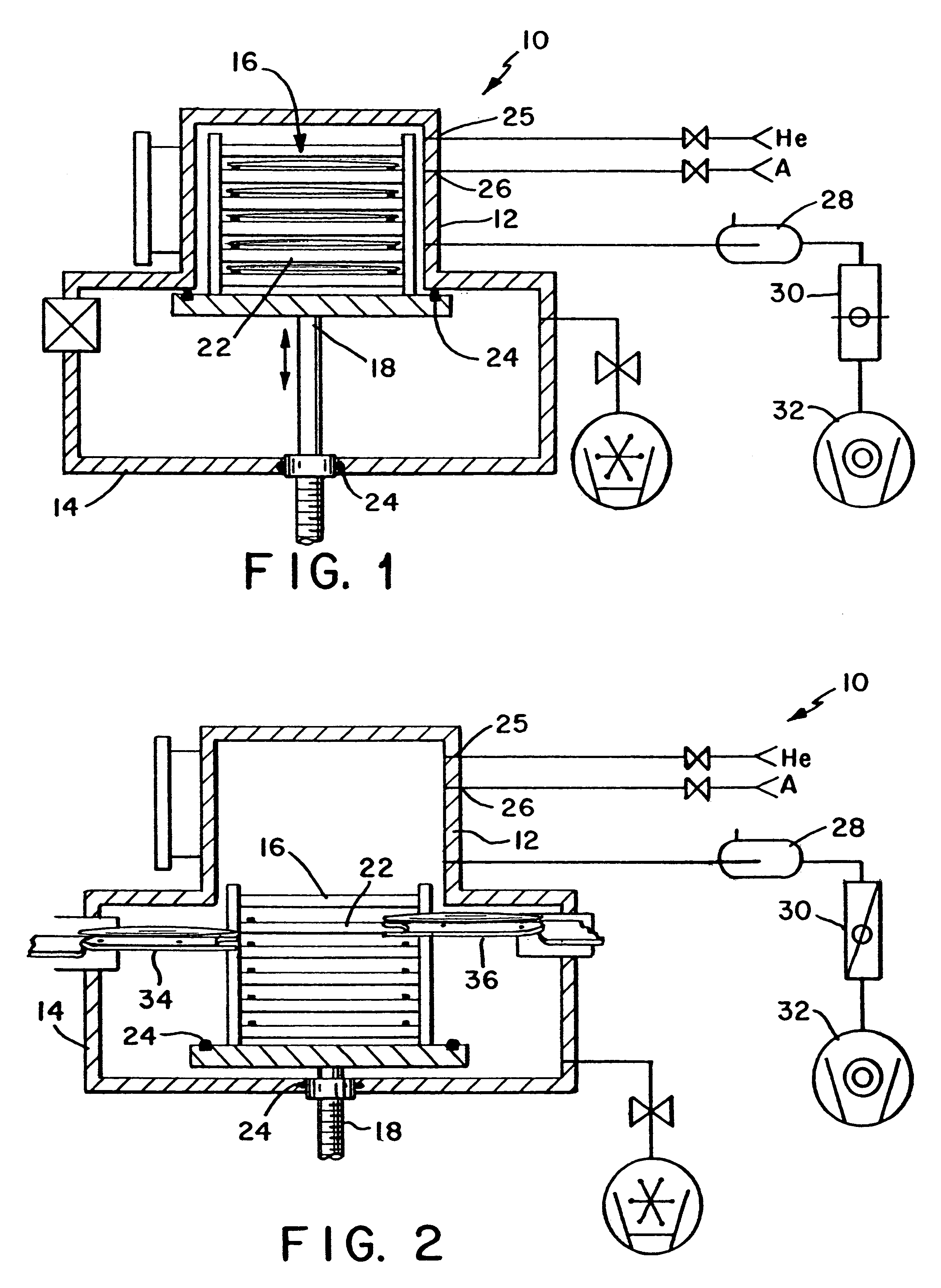
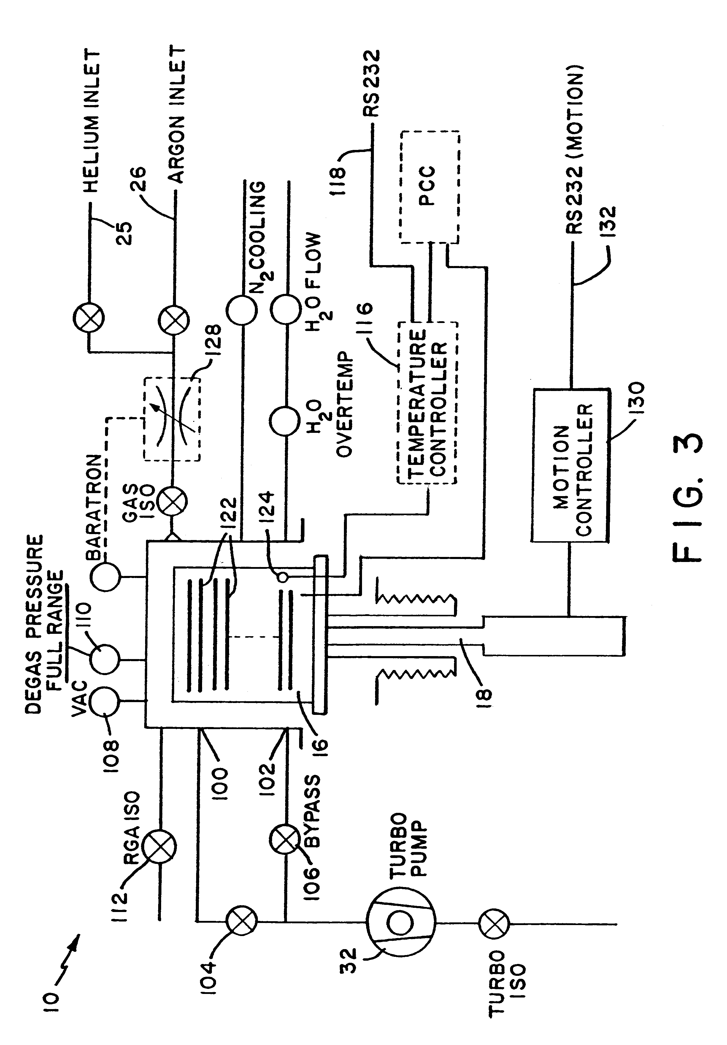
In describing the preferred embodiment of the present invention, reference will be made herein to FIGS. 1-6 of the drawings in which like numerals refer to like features of the invention.

This invention describes an apparatus and process to improve wafer throughput in cluster tools by using a multi-level shelf degas station. The process is sequential and divides up the total degassing time for each wafer over a number of cycles. This has two advantages over a batch system. First, by dividing the process into cycles that are defined by the desired throughput cycle time, higher throughput is achieved. Second, each wafer is sequenced through the degas process in the same manner so that the process remains consistent. By utilizing a pass-through configuration that is accessed by more than one robotic arm, the apparatus allows for simultaneous exchanges and does not require a station to be completely unloaded before reloading. In addition, because the apparatus is a pass-through configur...


PUM

PropertyMeasurementUnit
Internal pressureaaaaaaaaaa
Temperatureaaaaaaaaaa
Fractionaaaaaaaaaa

Abstract

A multi-level shelf degas station relying on at least two heaters integrated within wafer holding shelves or slots, where the semiconductor wafers do not have direct contact with the heater shelves. The heaters provide conduction heating. In order to degas a wafer, the heater and wafer holder assembly is positioned in a sequential manner through each wafer slot to the next available slot. If a degassed wafer exists in the slot, a transfer chamber arm removes it. A loader arm then places a wafer in the available, empty slot and the stage is moved upwards to receive the wafer from the loader arm. The transfer chamber arm removes an individual wafer from the heater and wafer holder assembly allowing the removed wafer to be individually processed while the other wafers remain in the heater and wafer holder assembly. In some instances, a loader arm may also remove wafers. The remaining wafers in the heater and wafer holder assembly are subjected to further degas treatment while the wafer(s) removed by the transfer chamber arm are exposed to other process steps. Air-cooling chambers are employed to facilitate cooling the wafer slots for ease of removal and maintenance.

Description

1. Field of the InventionThe present invention relates to an apparatus and method for manufacturing integrated circuits. More specifically, the present invention relates to an apparatus and method to enhance wafer throughput in semiconductor device processing.2. Description of Related ArtPre-processing is commonly performed on semiconductor wafers to remove surface and absorbed impurities such as water vapor and other gases from the silicon wafers. If left to reside on and within the wafer, these impurities may result in defects in the integrated circuit. It has been established that gases and water vapor may be removed from the wafers by heating or baking the wafer at some elevated, predetermined temperature in a vacuum for a specified period of time.Current wafer processing tools have focused on batch processing of multiple wafers, utilizing a single robotic arm for insertion and removal of the wafers from their holder or cassette. The wafers undergo radiated heat treatment in bat...

Claims


Application Information

Patent Timeline
IPC IPC(8): H01L21/67H01L21/00H01L21/677
CPCH01L21/67017H01L21/67757Y10T29/41Y10S438/908Y10S438/909
Inventor BARBER, KENNETH K.FISSEL, MARKJOH, SOO YUNKHOSLA, MUKULLEVY, KARL B.MARTINSON, ROBERTMEYERS, MICHAELSHRIVASTAVA, DHAIRYA
Owner NOVELLUS SYSTEMS
Why Eureka
Try Eureka