Method of reducing sub-threshold leakage in circuits during standby mode

a technology of standby mode and sub-threshold current, which is applied in the direction of logic circuits, pulse techniques, digital storage, etc., can solve the problems of reducing the performance of the circuit, increasing the size of the circuit, and reducing the power requirements of the integrated circuit, so as to and minimize or reduce the sub-threshold current leakage

Inactive Publication Date: 2003-02-18
INFINEON TECH AG +1
View PDF2 Cites 39 Cited by
  • Summary
  • Abstract
  • Description
  • Claims
  • Application Information

AI Technical Summary

Benefits of technology

The device coupled to the output node to set the output node to a potential which minimizes the sub-threshold leakage may comprise a PFET transistor coupled between the upper power rail and the output node which, upon receipt of a standby signal, maintains the potential of the output node at the potential of the upper power rail. Alternatively, the device comprises an NFET transistor coupled between the lower power rail and the output node which, upon receipt of a standby signal, maintains the potential of the output node at the potential of the lower power rail.
FIG. 12 is a circuit diagram embodying an nineth embodiment of the present invention which minimizes or reduces sub-threshold current leakage.

Problems solved by technology

If this type of circuit is frequently used on an integrated circuit chip with wiring at the sub-micron level, the sub-threshold leakage could be in the range of microamperes, which is considered excessive.
This circuit requires an additional device N2, which has a higher threshold voltage than transistor N2, and therefore has the disadvantage of resulting in increased size and degraded performance if the circuit is used to drive a bus.
This solution is undesirable since it has increased power dissipation associated with the larger voltage swing (from V.sub.NEG to V.sub.DD) at node A. Accordingly, there exists a long-felt need for a method to reduce the amount of sub-threshold leakage associated with circuits utilizing low threshold devices and thereby reduce standby or sleep mode current leakage.

Method used


Image

  • Method of reducing sub-threshold leakage in circuits during standby mode
  • Method of reducing sub-threshold leakage in circuits during standby mode
  • Method of reducing sub-threshold leakage in circuits during standby mode

Examples


first embodiment

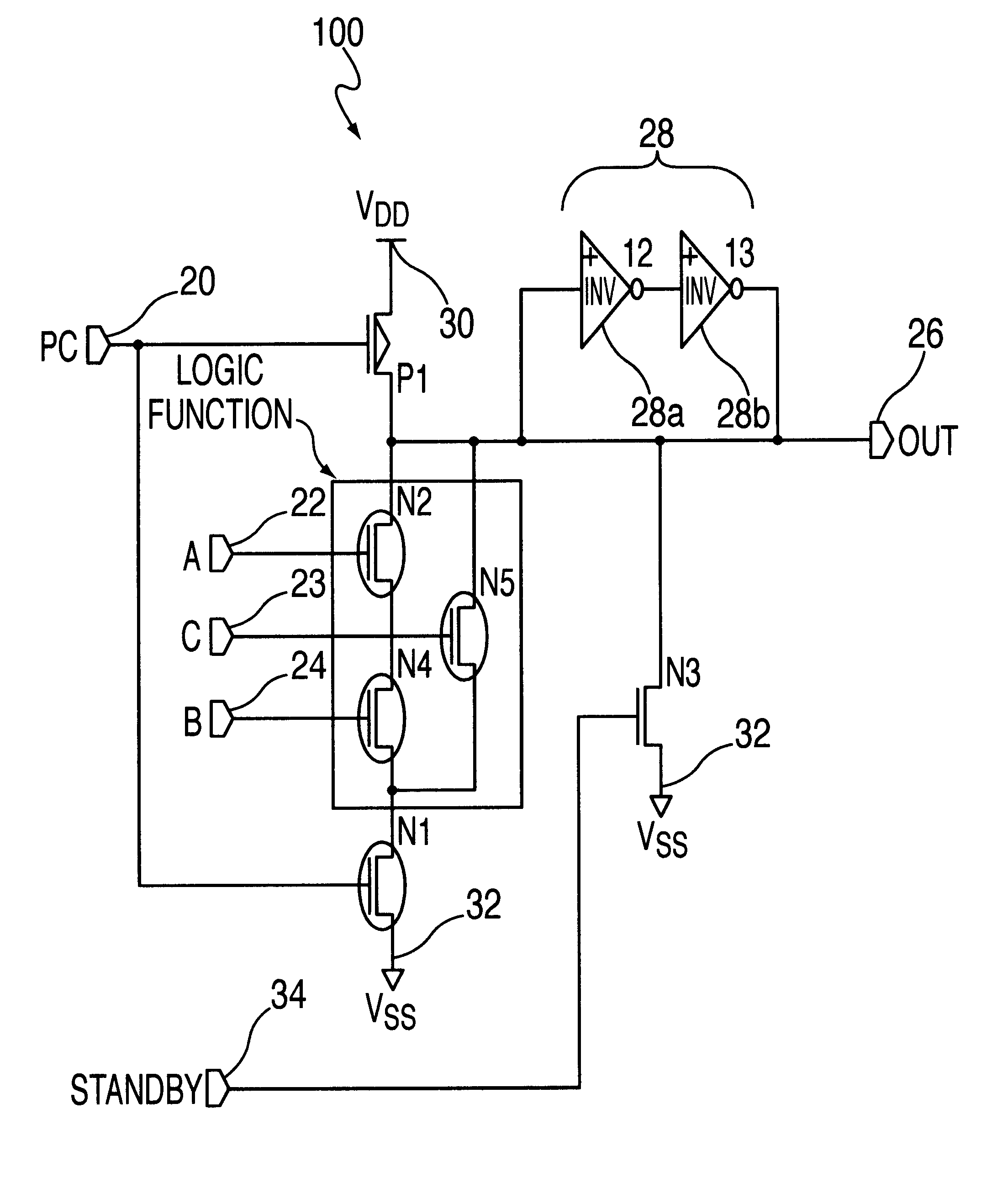
FIG. 4 shows the present invention, which adds to a dynamic logic circuit 100 of the type used in a DRAM a device to discharge the output node to ground during standby mode. This dynamic logic circuit performs an AND-OR-INVERT logical operation (i.e., INPUT=A, B, C, OUTPUT=INVERT (A AND B OR C)) The circuit operates in a manner similar to that of FIG. 2, wherein transistor P1 is connected to the upper power rail 30 at V.sub.DD and the output at node 26 is precharged to V.sub.DD (logic level 1) by a negative active pulse PC applied at precharge node 20 coupled to the transistor P1 gate and to the transistor N1 gate. This occurs when pulse PC, initially at V.sub.DD (logic level 1) drops to Vss (logic level 0) at ground 32 for a predetermined time, e.g., 2-5 nanoseconds, and then returns to V.sub.DD and logic level 1. During the time pulse PC is at level 0, transistor P1 conducts and charges output node 26 to logic level 1, which in turn sets latch 28, made up of inverters I228a and 13...

second embodiment

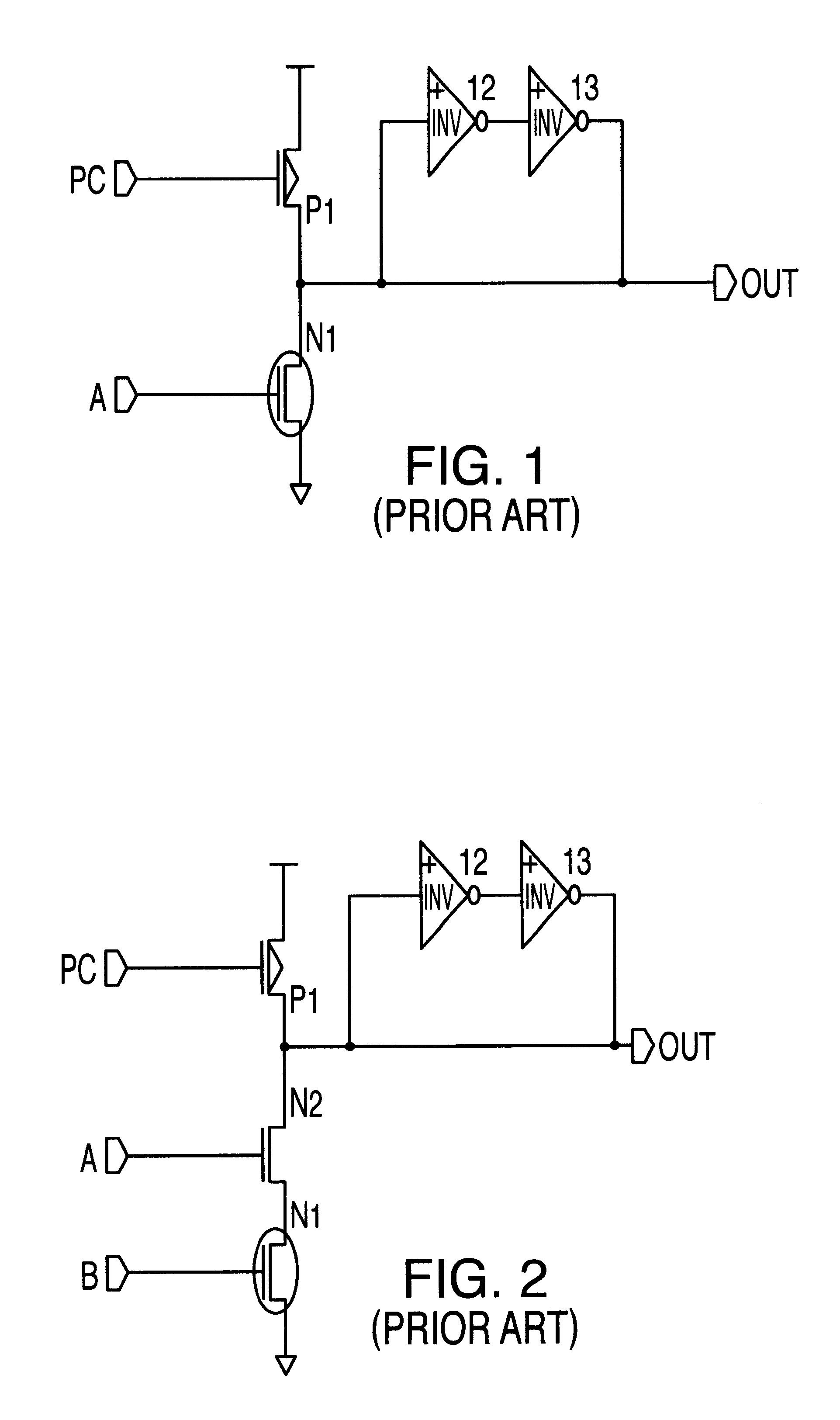
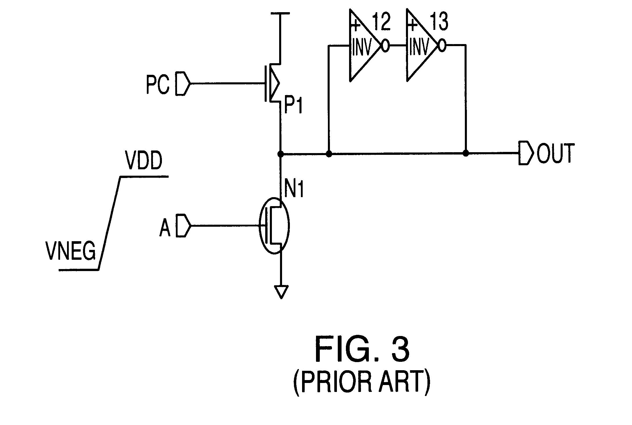
FIG. 5 shows the present invention, which adds to a dynamic receiver 105 of the type used in a DRAM a device to discharge the output node to ground during standby mode. The circuit operates in a manner similar to that of FIG. 2, wherein transistor P1 is connected to the upper power rail 30 at V.sub.DD and the output at node 26 is precharged to V.sub.DD (logic level 1) by a negative active pulse PC applied at precharge node 20 coupled to the transistor P1 gate. This occurs when pulse PC, initially at V.sub.DD (logic level 1) drops to V.sub.SS (logic level 0) for a predetermined time, e.g., 2-5 nanoseconds, and then returns to V.sub.DD and logic level 1. During the time pulse PC is al level 0, transistor P1 conducts and charges output node 26 to logic level 1, which in turn sets latch 28, made up of inverters I228a and I328b, to hold logic level 1. The circuit then waits for addresses or signals at A 22 and B 24 to be asserted during the evaluation phase. The drain of standard thresho...


PUM


Abstract

A dynamic logic circuit having reduced sub-threshold leakage current during standby mode comprises a connection to at least one upper power rail, a connection to a lower power rail, a precharge node, and an output node adapted to be charged to the potential of the upper power rail after a precharge signal is received at the precharge node. A latch on the output node is provided to maintain the potential at the output node, along with at least one input node for receiving at least one evaluation signal to maintain the potential at the output node to the voltage of the upper power rail or reduce the potential at the output node to the potential of the lower power rail. A device is coupled to the output node to set the output node to a potential which minimizes the sub-threshold leakage upon receipt of a standby signal to maintain the potential at the output node at the potential of the upper power rail or at the potential of the lower power rail.

Description

1. Field of the InventionThis invention relates to integrated circuits and, in particular, to power requirements of integrated circuit chips.2. Description of Related ArtIntegrated circuit chips have power requirements which become increasingly critical as the trend continues toward making circuits smaller and more dense, and operating such devices from battery power. There is constant motivation to reduce chip power usage due to packaging requirements, as well as applications in portable devices which have limited battery power.A typical prior art low voltage dynamic circuit is shown in FIG. 1. This dynamic logic circuit performs the INVERT logical operation (i.e., INPUT=A, OUTPUT=A) In operation of the circuit, a negative active pulse, PC is initially provided at the gate of transistor P1 to precharge the output node, OUT, to VDD. The voltage at node OUT is held high by the latch formed by inverters I1 and I3. When input signal A rises to a low voltage logic level 1, the node OUT ...

Claims


Application Information

Patent Timeline
Patent Type & Authority Patents(United States)
IPC IPC(8): H03K19/00H03K19/096G11C11/407
CPCH03K19/0963H03K19/0016G11C11/407
Inventor HANSON, DAVID R.KIRIHATA, TOSHIAKIMUELLER, GERHARD
Owner INFINEON TECH AG
Why Eureka
Try Eureka