

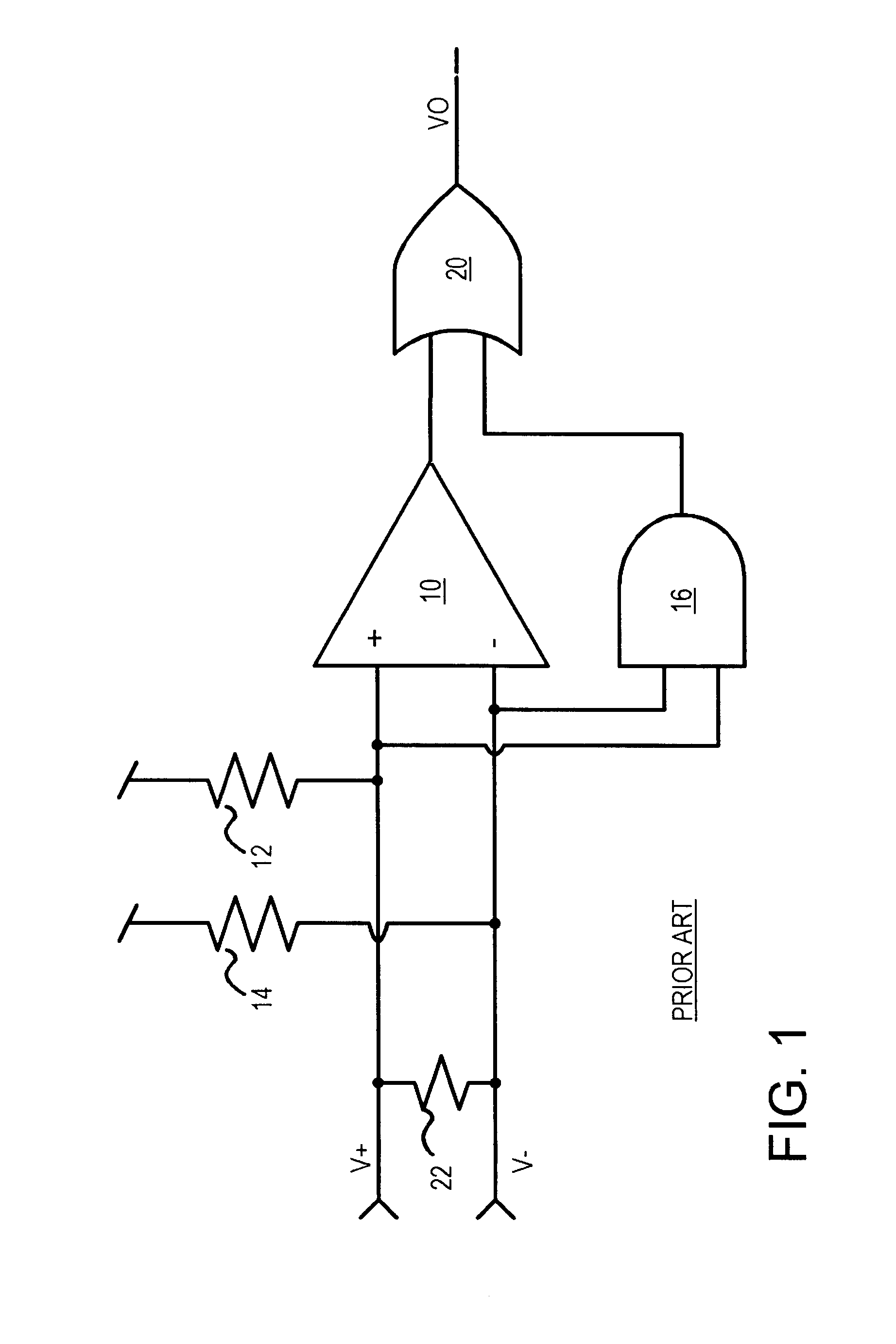
Fail-safe circuit with low input impedance using active-transistor differential-line terminators
a technology of active-transistor differential and low input impedance, applied in the field of differential receivers, can solve the problems of large signal swing, low signal quality, and low signal quality, and achieve the effects of reducing data quality and transmission rate, increasing system noise, and increasing electro-magnetic interference (emi)
- Summary
- Abstract
- Description
- Claims
- Application Information
AI Technical Summary
Problems solved by technology
Method used
Image

Examples
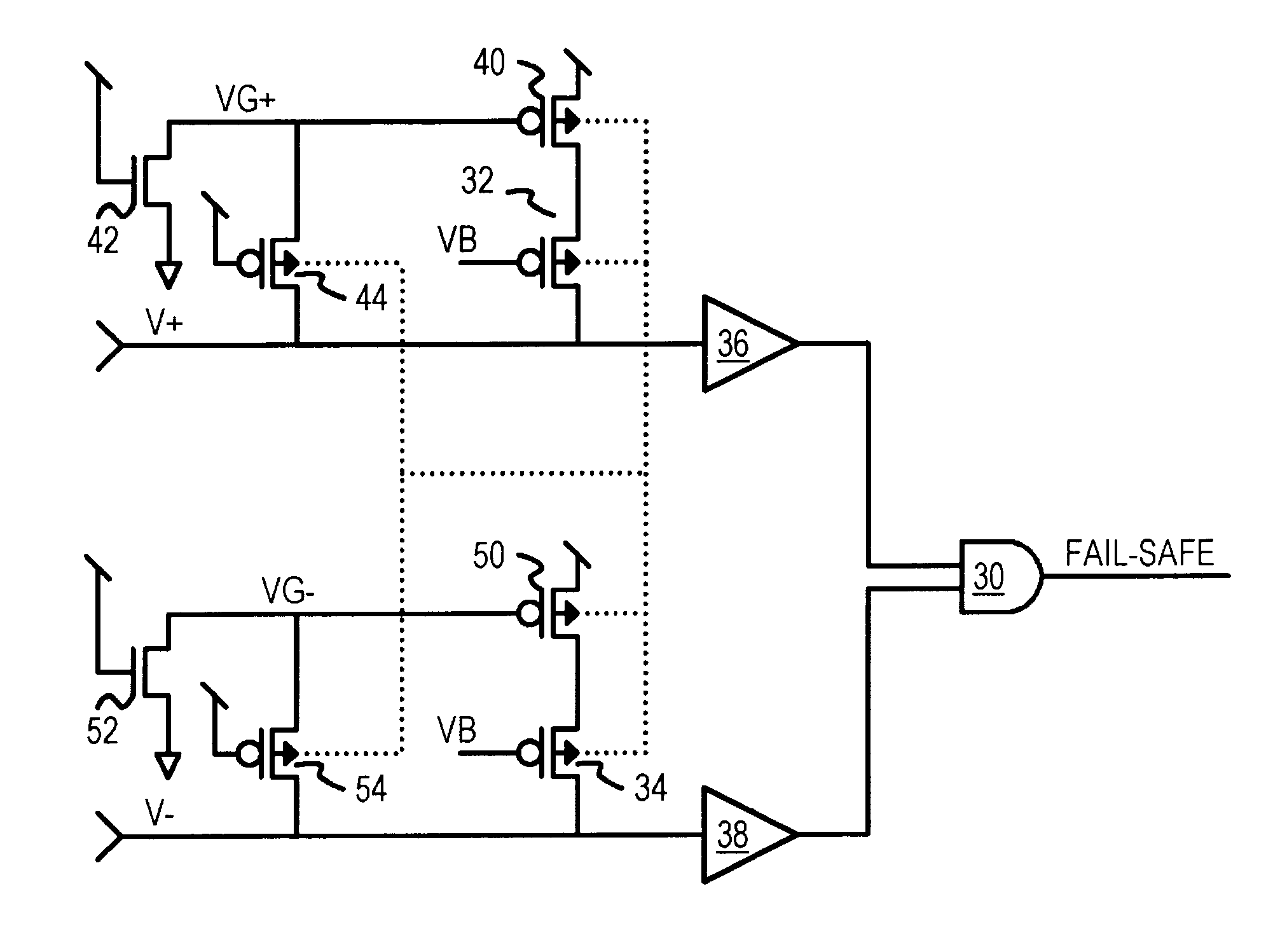
Embodiment Construction
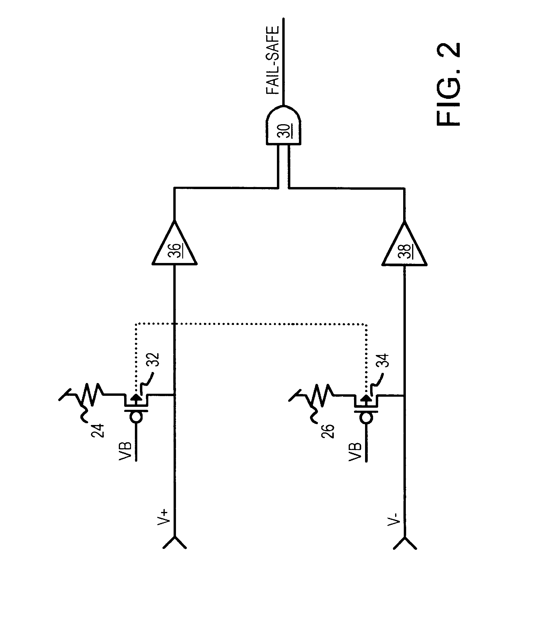
Several other embodiments are contemplated by the inventors. For example many different transistor sizes could be used, and additional transistors and components such as logic gates, capacitors and resistors could be added. Many different resistance values can be used, and the load or terminating resistor is normally selected to match the impedance of the V+, V- transmission lines, usually in the range of 50 to 120 Ohms. Various inversions in the logic can be introduced, and NAND gates rather than NOR gates can be substituted using DeMorgan's theorem. The inverting and non-inverting inputs to the comparators and the differential amplifier can be swapped to invert their outputs. Active-low signals rather than active-high signals can be substituted. Several gates can be combined into a larger gate, such as a 3-input AND or NAND gate.
Pull-down resistors rather than pull-up resistors could be attached to the differential inputs, and n-channel rather than p-channel transistors could be p...
PUM
 Abstract
Description
Claims
Application Information