Charge pump circuit

a charge pump and circuit technology, applied in the direction of power conversion systems, instruments, dc-dc conversion, etc., can solve the problems of significant power consumption, increased die size, and increased cos

Inactive Publication Date: 2003-02-25
SANDISK TECH LLC
View PDF10 Cites 117 Cited by
  • Summary
  • Abstract
  • Description
  • Claims
  • Application Information

AI Technical Summary

Problems solved by technology

While on-chip voltage generator circuits may relieve a user from supplying a second power supply voltage, such circuits frequently require a significant amount of layout area to implement, which may increase die size substantially, and consequently increase costs.
Moreover, such voltage generator circuits also may consume a significant amount of power relative to the remainder of the circuit, and thus increase the current that must be supplied by the user (e.g., by the VDD power supply).
Any increase in power dissipation may also increase the temperature of the die during operation.
In a battery-powered environment, any increase in power consumed by a device may have significant implications for battery life, and any additional heat generated may also be difficult to dissipate.

Method used


Image

  • Charge pump circuit
  • Charge pump circuit
  • Charge pump circuit

Examples


Embodiment Construction

)

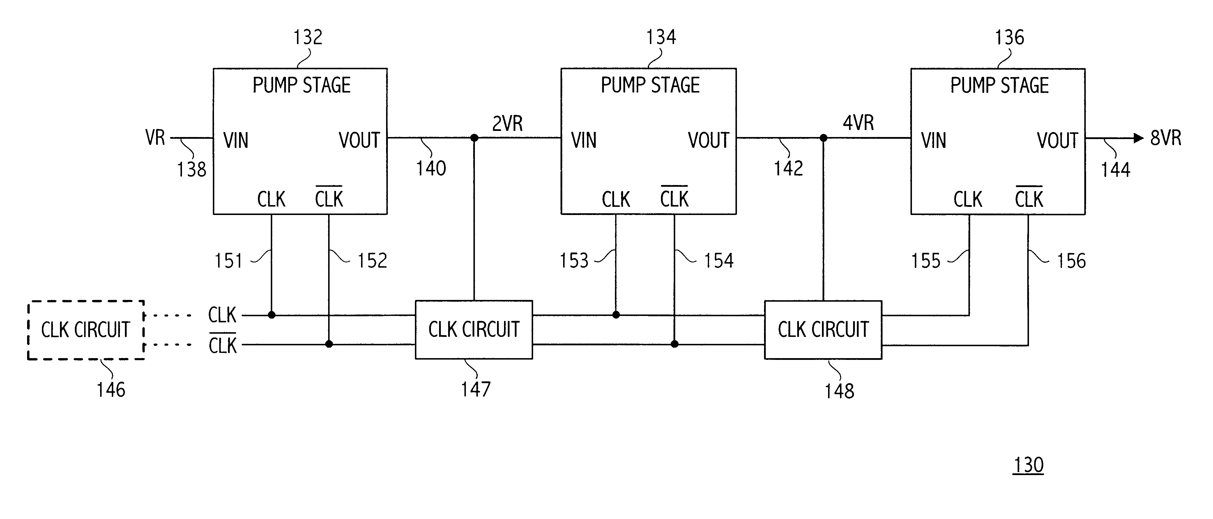
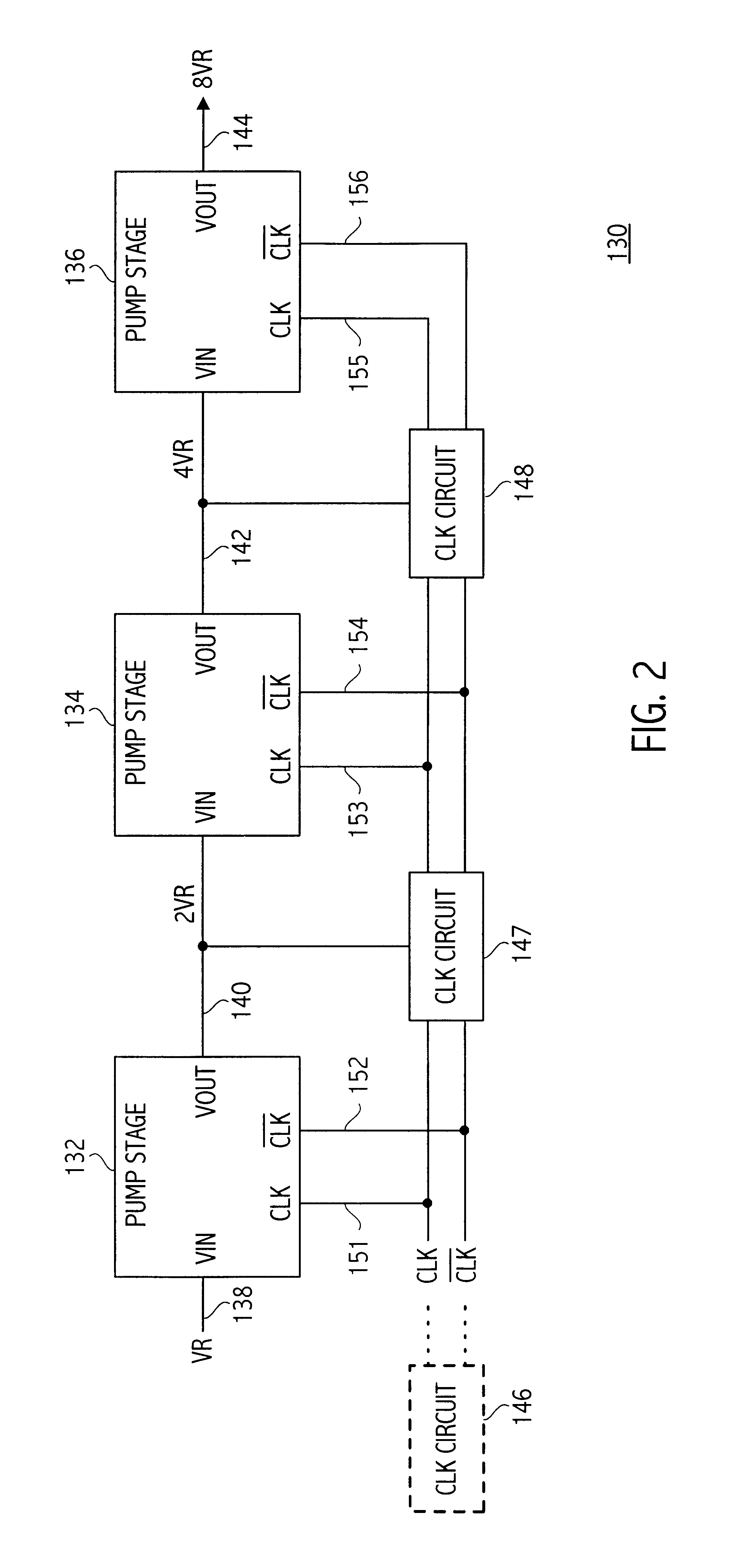
Referring now to FIG. 2, a block diagram is shown of an improved charge pump in accordance with a preferred embodiment of the present invention. The charge pump circuit 130 includes three serially-connected charge pump stages 132, 134, and 136. Each pump stage is contemplated to be identical or similar to the other two, although such is not required, and the three charge pump stages may be sized non-identically, as further described below. While the charge pump circuit 130 is shown utilizing three such charge pump stages, it should become clear that lesser or greater numbers of charge pump stages are also contemplated.

An input voltage, here denoted as having a magnitude VR, is conveyed on node 138 to a VIN input of the first charge pump stage 132. A complementary pair of clock signals CLK and / CLK are conveyed respectively on nodes 151 and 152 to corresponding complementary clock inputs of the charge pump stage 132. These CLK and / CLK signals may be generated by a clock circuit 146...


PUM


Abstract

A charge pump circuit includes, in a preferred embodiment, a plurality of serially-connected pump stages, each of which is driven by one or more associated clock signals for the stage. The amplitude of the clock signals associated with a respective one of the pump stages differ in amplitude from that of the clock signals associated with at least one other pump stage. As a result, the additional voltage achieved by each successive pump stage may be progressively larger for each successive pump stage. An exemplary charge pump circuit provides clock signals which increase in amplitude with each successive pump stage, and provides with each successive pump stage an output voltage having a magnitude that is a multiplicative factor of the magnitude of the input voltage for the stage. Consequently, the output voltage achieved by the exemplary charge pump circuit is an exponential function of the number of pump stages within the charge pump circuit.

Description

1. Field of the InventionThe present invention relates to semiconductor voltage generator circuits, and particularly to capacitive voltage multiplier circuits.2. Description of the Related ArtMany integrated circuits, particularly those using a single power supply voltage, incorporate on-chip circuitry to generate a "boosted" voltage having a magnitude greater than the power supply voltage. Frequently this boosted voltage is used as a veritable power supply voltage for portions of the circuitry contained on the integrated circuit. For example, certain types of semiconductor memories, such as "flash" EEPROM memories, write a memory cell by accelerating electrons across a tunneling dielectric and storing the charge on a floating gate above a field effect transistor. On contemporary devices, this acceleration of charge across the tunneling dielectric frequently requires a "write voltage" on the order of 8 volts, yet the remainder of the operations of the memory circuitry typically requ...

Claims


Application Information

Patent Timeline
Patent Type & Authority Patents(United States)
IPC IPC(8): H02M3/04H02M3/07
CPCH02M3/073
Inventor JOHNSON, MARK G.NOLAN, III, JOSEPH G.CROWLEY, MATTHEW P.
Owner SANDISK TECH LLC
Why Eureka
Try Eureka