CMOS integrated circuit having PMOS and NMOS devices with different gate dielectric layers

a technology of dielectric layer and integrated circuit, which is applied in the direction of semiconductor devices, electrical equipment, transistors, etc., can solve the problem that the manufacturing of cmos integrated circuits is generally more difficul

Inactive Publication Date: 2003-03-25
INTEL CORP
View PDF29 Cites 91 Cited by
  • Summary
  • Abstract
  • Description
  • Claims
  • Application Information

AI Technical Summary

Problems solved by technology

Although CMOS integrated circuits are generally more difficult to manufacture because they contain both PMOS and NMOS devices on a single substrate, CMOS devices are necessary in order to reduce power consumption, especially in very large scale (VLSI) circuits such as microprocessors where literally millions of transistors are coupled together.

Method used


Image

  • CMOS integrated circuit having PMOS and NMOS devices with different gate dielectric layers
  • CMOS integrated circuit having PMOS and NMOS devices with different gate dielectric layers
  • CMOS integrated circuit having PMOS and NMOS devices with different gate dielectric layers

Examples


Embodiment Construction

A novel CMOS integrated circuit having PMOS and NMOS devices with different gate dielectric layers is described. In the following description numerous specific details are set forth, such as specific materials, dimensions, and processes, in order to provide a thorough understanding of the present invention. It will be obvious, however, to one skilled in the art that the present invention may be practiced without these specific details. In other instances, well known semiconductor equipment and processes have not been described in particular detail in order to avoid unnecessarily obscuring the present invention.

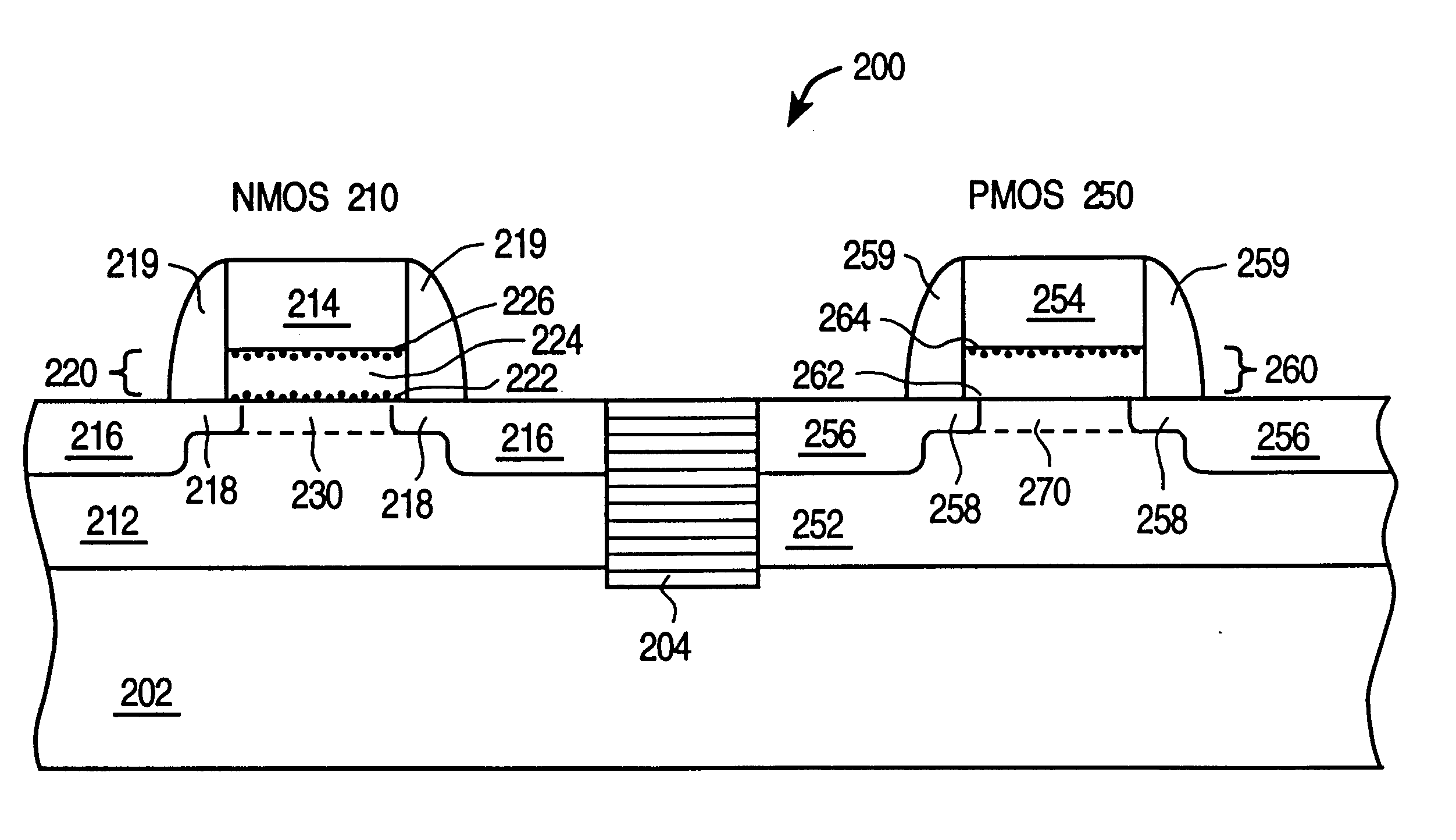
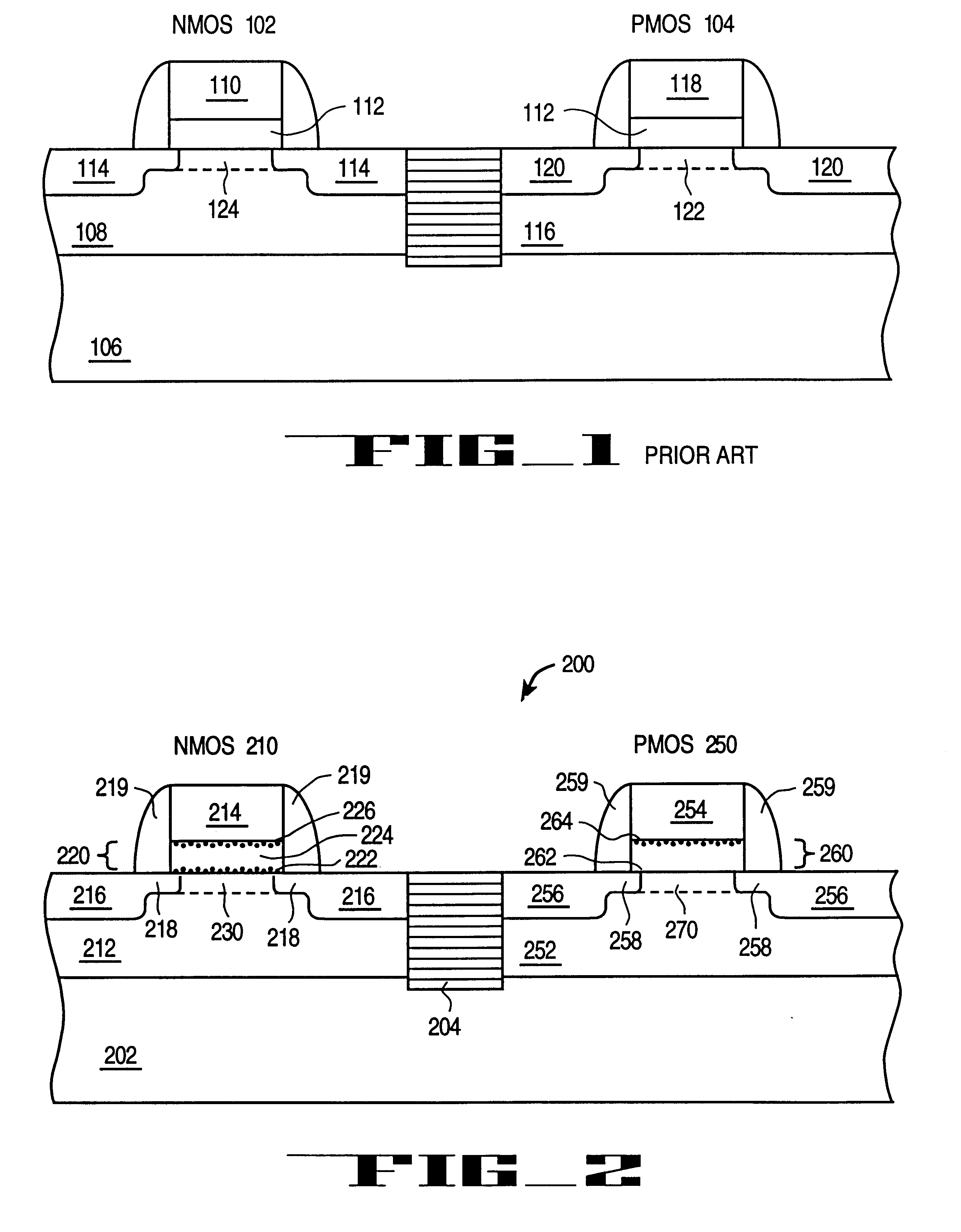
The present invention is a novel CMOS integrated circuit. According to the present invention, the PMOS transistors have a gate dielectric layer with dielectric properties which optimize the performance and reliability of the PMOS transistor, while the NMOS transistors have a gate dielectric layer with dielectric properties, different than the PMOS transistors', which optimize ...


PUM


Abstract

A CMOS integrated circuit having a PMOS and NMOS device with different gate dielectric layers. According to the present invention, an NMOS transistor is formed on a p-type conductivity region of a semiconductor substrate. The NMOS transistor has first gate dielectric layer formed on the p-type conductivity region. A PMOS transistor is formed on a n-type conductivity region of the semiconductor substrate. The PMOS transistor has a second gate dielectric layer wherein the second gate dielectric layer has a different composition than the first gate dielectric layer.

Description

1. Field of the InventionThe present invention relates to the field of semiconductor integrated circuits and more specifically to a CMOS integrated circuit wherein the PMOS and NMOS transistors have different dielectric properties.2. Discussion of Related ArtComplimentary metal oxide semiconductor (CMOS) integrated circuits are widely used in logic applications such as in the design of very large scale integrated circuits such as microprocessor and microcontrollers.As shown in FIG. 1, a CMOS integrated circuit 100 contains both n-type MOS (NMOS) transistors and p-type MOS (PMOS) transistors formed on a single substrate 106. NMOS device 102 is formed on a p-type conductivity region 108 of substrate 106 and contains a gate electrode 110 formed on a gate dielectric gate layer 112 and a pair of n-type source / drain regions 114 formed on laterally opposite sides of gate electrode 110. Similarly, PMOS device 104 is formed on a n-type conductivity region 116 of substrate 106 and contains th...

Claims


Application Information

Patent Timeline
Patent Type & Authority Patents(United States)
IPC IPC(8): H01L21/70H01L21/8238H01L27/085H01L27/092
CPCH01L27/0922H01L21/823857
Inventor CHAU, ROBERT S.
Owner INTEL CORP
Why Eureka
Try Eureka