

Image processing device and image processing method
a technology of image processing and image processing, applied in the field of image processing device and image processing method for computer graphics, can solve the problems of large processing involved, poor processing efficiency, and long processing tim
- Summary
- Abstract
- Description
- Claims
- Application Information
AI Technical Summary
Benefits of technology
Problems solved by technology
Method used
Image

Examples
embodiment 1
of the Invention
Below, a device and method according to a first embodiment are described.
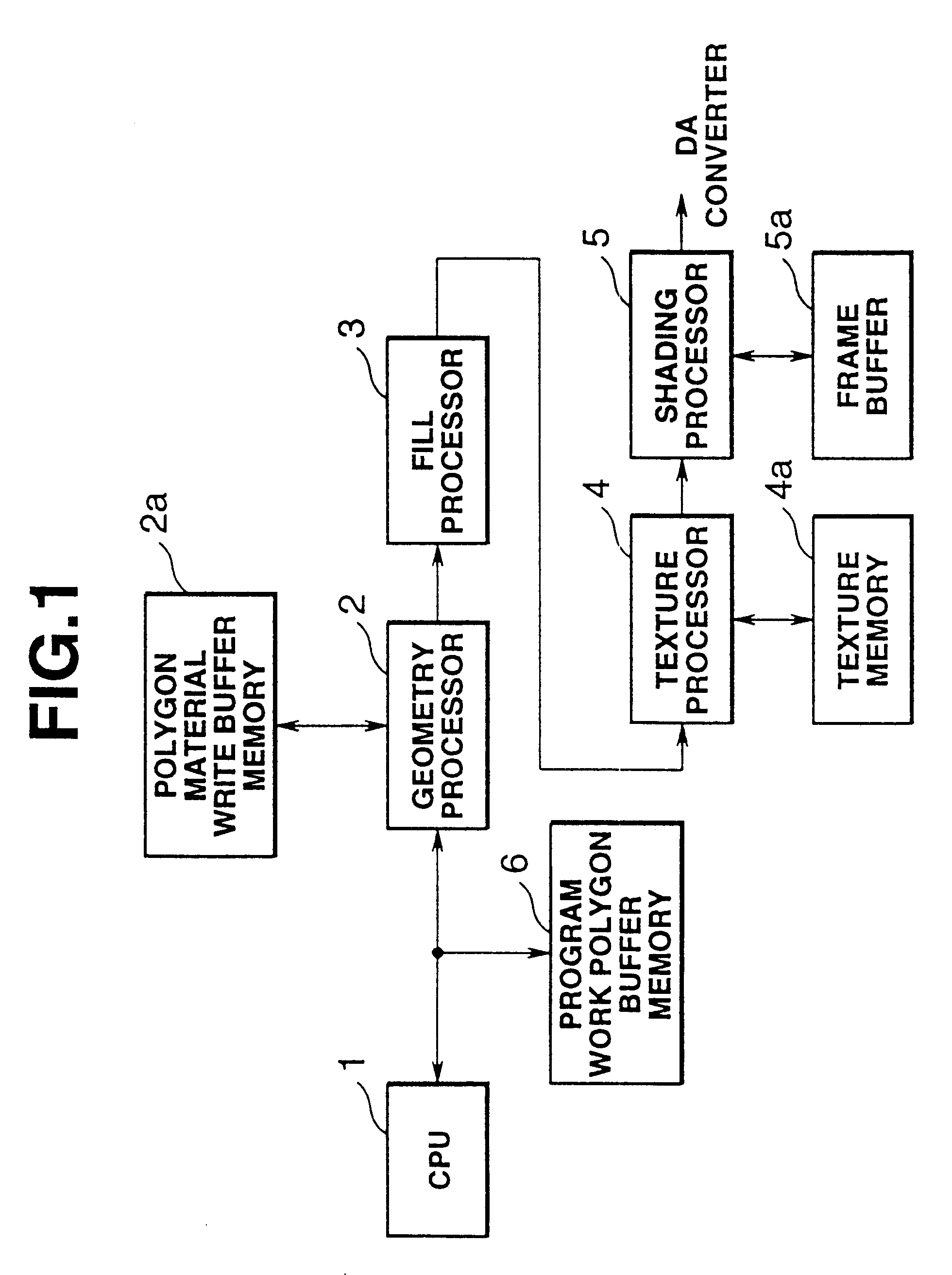
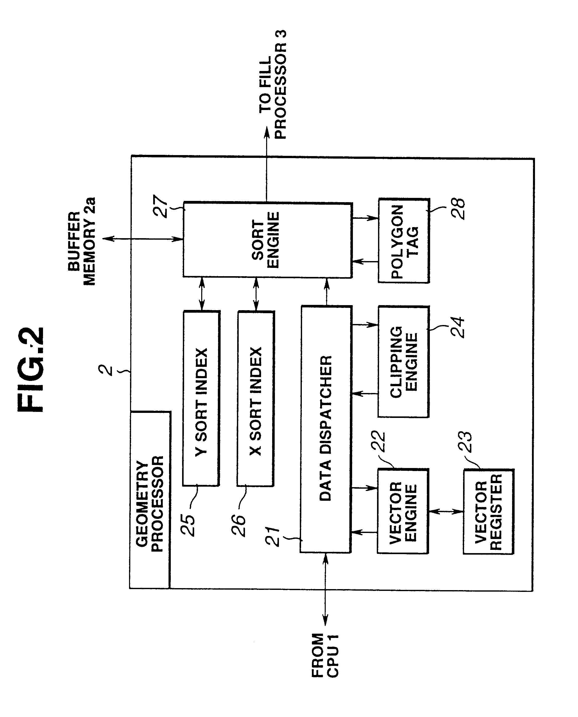
FIG. 1 is an approximate functional block diagram of an image processing device relating to the first embodiment. In the drawing, 1 is a CPU (central processing unit), which implements various control functions, by performing operations relating to objects in a virtual space, obtaining information therefor, and the like. 2 is a geometry processor, which performs geometric transformations (vector calculations), such as co-ordinates transformation, clipping, and perspective transformation, as well as intensity transformation, relating to polygons in three-dimensional computer graphics. 2a is polygon material light buffer memory (polygon material light buffer RAM), which stores valid polygon data, material data and light data for one frame, when the geometry processor 2 is processing data. A `polygon` is a polyhedral object used to compose a three-dimensional figure in a virtual space. The contents...
embodiment 2
of the Invention
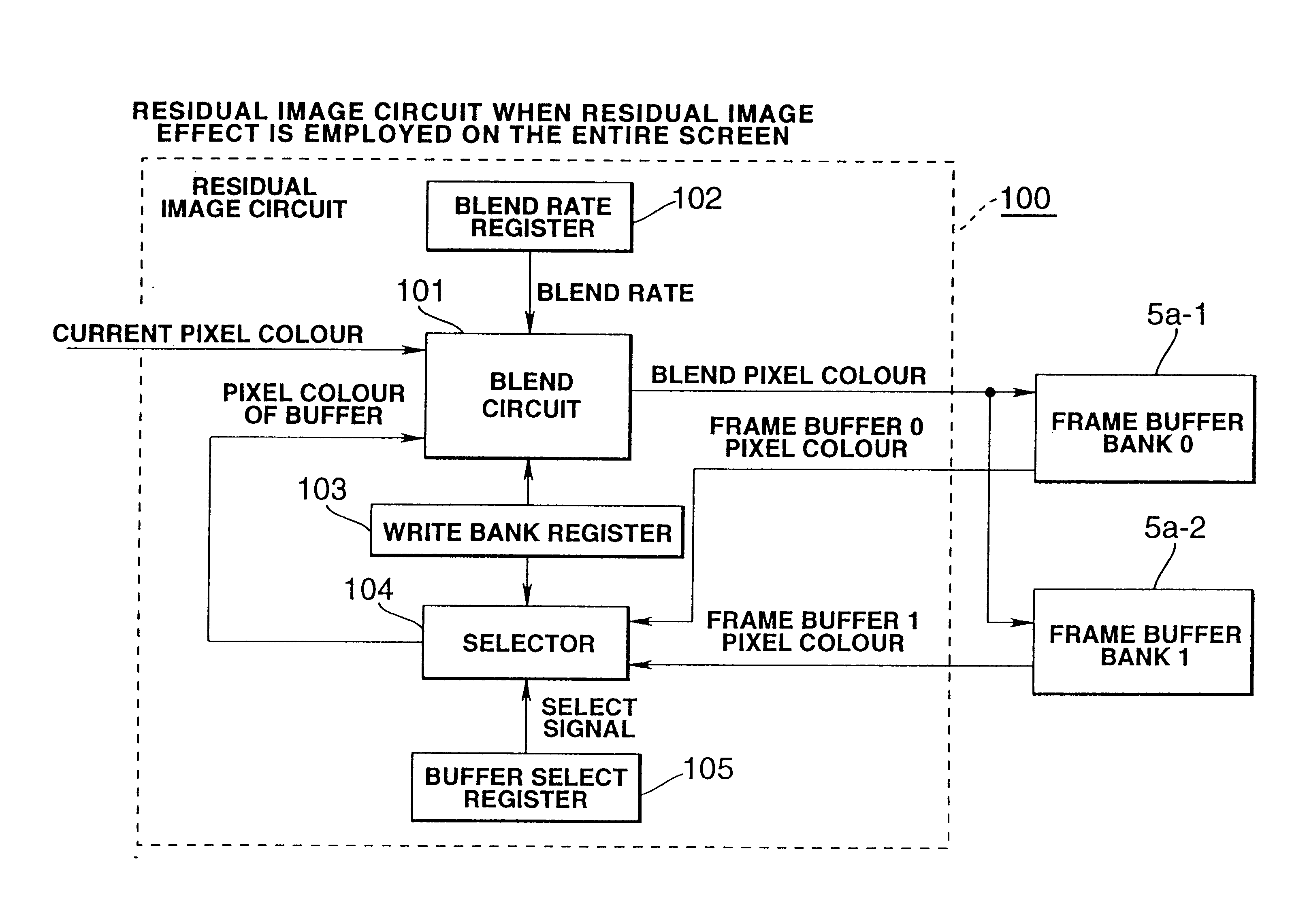
A residual image circuit according to this embodiment 2 is shown in FIG. 8. This Figure is a functional block diagram of a residual image circuit when a residual image effect in polygon units is employed.
In comparison with the residual image circuit of FIG. 6, the residual image circuit of FIG. 8 differs in that it has blend rate and slope at pixel units. "Slope" is a parameter for attenuating the blend rate. To blend circuit 101, apart from the current pixel colour that is input from the outside, there is input a slope that expresses the difference of blend rate for the frame unit and blend rate for this pixel, through a selector 104 from residual buffers 5a-3, 5a-4. Residual image buffers 5a-3, 5a-4 store the blend rate and slope in correspondence with colour information of frame buffers 5a-1, 5a-2.
SUB block 106 of FIG. 8 is a circuit that finds the blend rate that is used by the next frame by subtracting the slope from the blend rate in residual image buffers 5a-3...
embodiment 3
of the Invention
A functional block diagram for actually implementing the layout of embodiment 1 of the invention is shown in FIG. 10.
In FIG. 10, colour buffer RAM 121 is RAM contained within shading circuit 120 and temporarily stores the colour data. For example, it stores the colour data of 8.times.8 pixels. Its interior is of a two-bank construction so that, when writing is being performed to one bank by means of shading circuit 120, transfer circuit 110 can access the other bank. For access, reading and writing can be performed simultaneously. The data are 32-bit data and RGBA are respectively 10, 10, 10, 2 bits.
Blend rate register 112 holds the rate when blending is effected of the colour of frame buffer RAM 150 and the colour of colour buffer RAM 121. For example in the case of 8-bit data, the value may take the values 0.about.FFh. It is incremented if the most-significant bit (MSB) is 1, and a blend rate of FIX 1,8 is assumed for 0 to 100 h.
Blend circuit 111 blends the read da...
PUM
 Abstract
Description
Claims
Application Information