Method of manufacturing a semiconductor memory device

a memory device and semiconductor technology, applied in the direction of semiconductor devices, electrical appliances, transistors, etc., can solve the problems of increasing the number of steps of a manufacturing process, unable to achieve effective gettering, and unable to achieve microminiaturization of an elemen

Inactive Publication Date: 2003-04-22
MITSUBISHI ELECTRIC CORP
View PDF3 Cites 177 Cited by
  • Summary
  • Abstract
  • Description
  • Claims
  • Application Information

AI Technical Summary

Problems solved by technology

However, because an insulator existed under the single crystalline silicon in such an SOI element, the heavy metal atoms could not diffuse toward a gettering site of the silicon substrate positioned under the insulator through the insulator, wherein effective gettering was not obtainable.
However, there were problems that the number of steps of a manufacturing process was increased because it was necessary to newly form polycrystalline silicon for gettering and microminiaturization of an element became difficult because the width of the element and/or the thickness of the element was increased by newly providing a region for gettering in single crystalline silicon and newly forming a film for gettering on the single crystalline silic

Method used


Image

  • Method of manufacturing a semiconductor memory device
  • Method of manufacturing a semiconductor memory device
  • Method of manufacturing a semiconductor memory device

Examples


embodiment 1

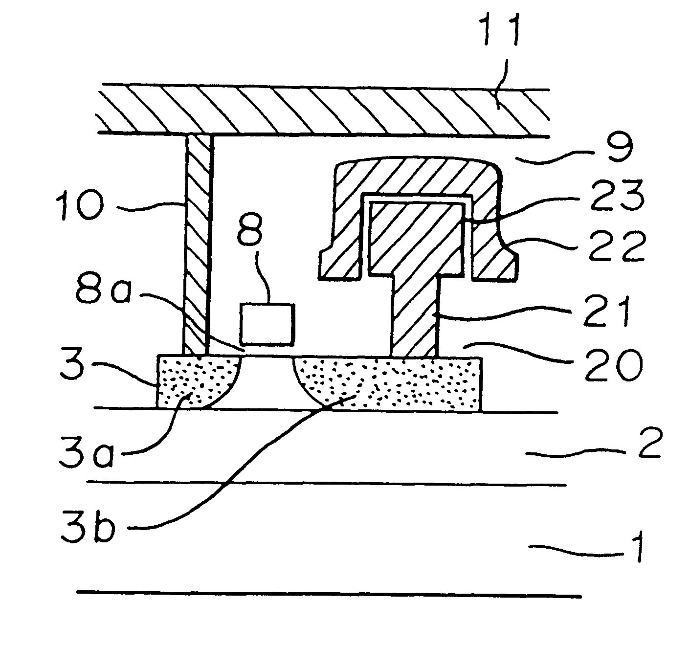
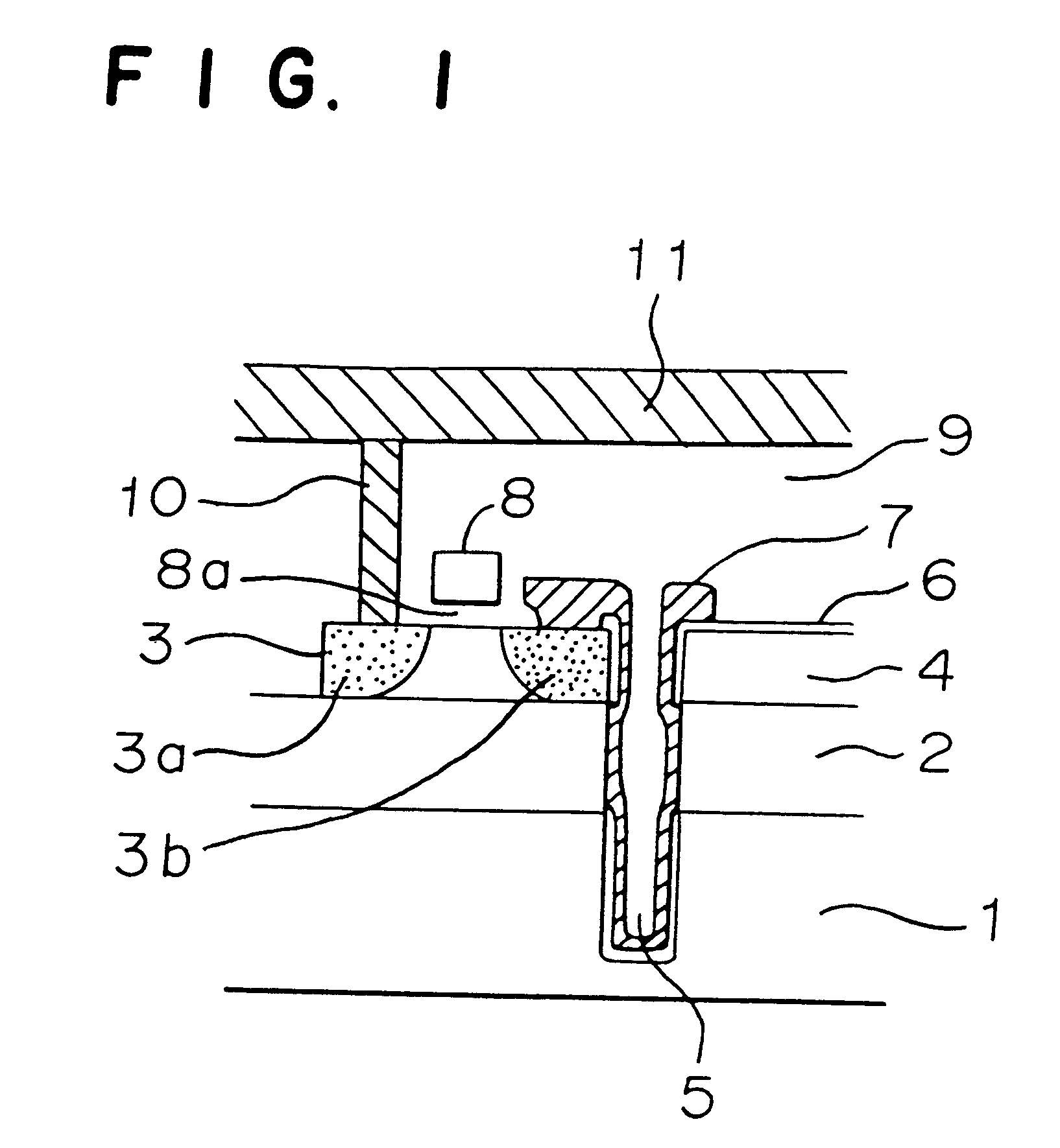
FIG. 1 is a cross-sectional view for schematically showing a semiconductor memory device of the present invention. As shown in FIG. 1, silicon on insulator (SOI) structure is adopted, wherein an insulator 2 made of silicon oxide (SiO.sub.2) is formed on a silicon substrate 1 and single crystalline silicon 3 (hereinbelow referred to as an SOI layer) is formed on the insulator 2.

On the SOI layer 3, source drain areas 3a and 3b of a MOSFET are formed and a gate oxide film 8a and a gate electrode 8 are sequentially provided between the source drain areas to thereby form the MOSFET. Meanwhile, it is possible to form an area having low concentration impurities, namely lightly doped drain (hereinbelow referred to as LDD) by injecting the low concentration impurities in ends of the source drain areas 3a and 3b.

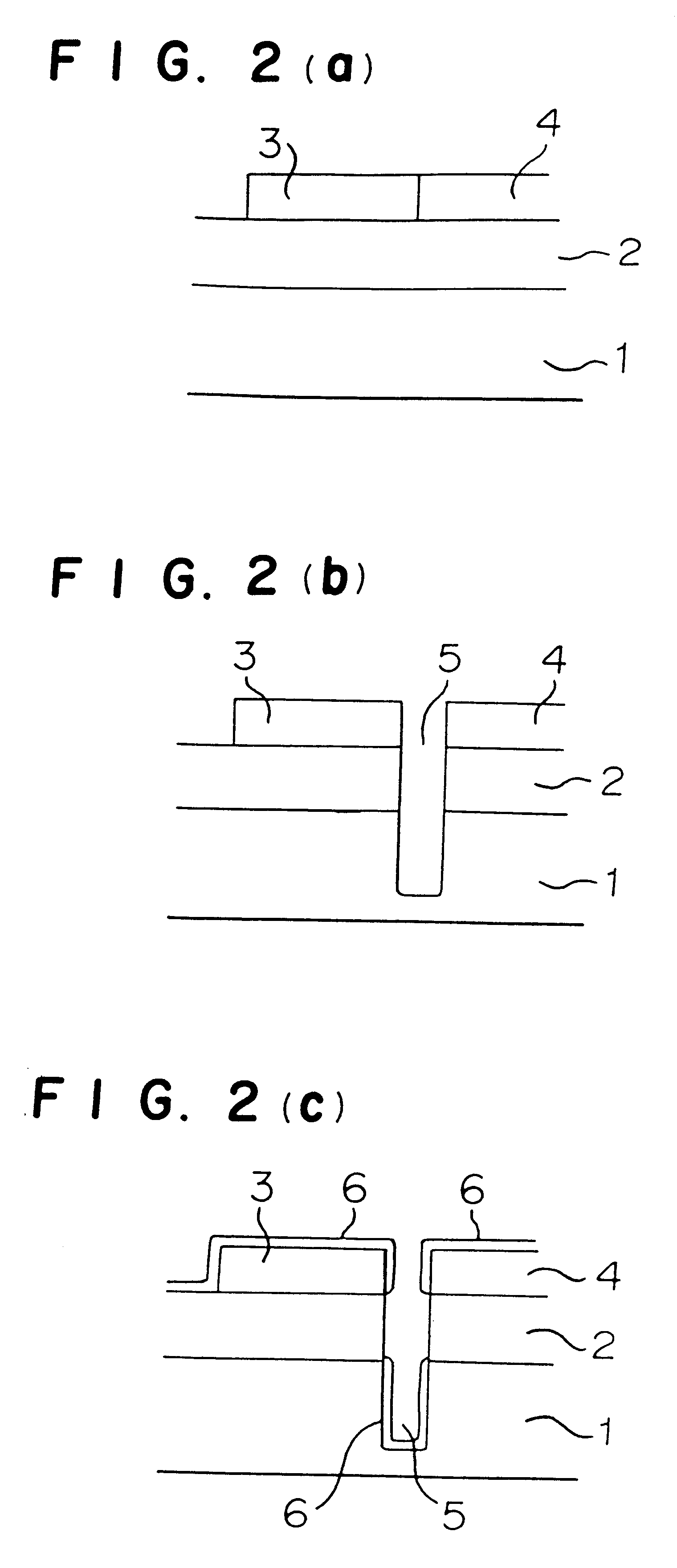
Further, a trench 5 is formed in a portion adjacent to the SOI layer; an insulating film 6 such as silicon oxide film is formed in an inner wall of the trench 5; and a polycrystallin...

embodiment 2

FIG. 4 is a cross-sectional view for schematically showing a semiconductor memory device according to Embodiment 2 of the present invention. In FIG. 1 concerning Embodiment 1 of the present invention, the polysilicon 7 to be the storage node is formed like a film on the silicon oxide film 6 in the inner wall of the trench 5. However, in the semiconductor memory device shown in FIG. 4, polysilicon 7 to be a storage node is embedded in the overall volume of a trench and formed like a plug. The other features are similar to those in FIG. 1 and therefore description is omitted.

In the next, a method of manufacturing the semiconductor memory device shown in FIG. 4 will be described. As for the method of manufacturing, the amount of depositing the polysilicon shown in FIG. 3b is increased in comparison with that of Embodiment 1 so that the polysilicon is sufficiently embedded in the trench. The following steps are similar to those in Embodiment 1 and therefore description is omitted.

Becaus...

embodiment 3

FIG. 5 is a cross-sectional view for schematically showing a semiconductor memory device according to Embodiment 3 of the present invention. In FIG. 1 concerning Embodiment 1, the gate electrode is formed so that the gate electrode is not formed on a portion for connecting the polysilicon 7 to be the storage node to the SOI layer 3. However, in the semiconductor memory device shown in FIG. 5, a gate electrode is formed so that a part of the gate electrode is formed in a portion for connecting a polysilicon 7 to be a storage node to an SOI layer 3. The other features are similar to those in FIG. 1 and therefore description is omitted.

In the next, a method of manufacturing the semiconductor memory device shown in FIG. 5 will be described. At a time of forming the polysilicon shown in FIG. 3b, one end of the polysilicon 7 connected to the SOI layer 3 is formed from an end portion of the SOI layer to a region corresponding to a gate electrode. Thereafter, the part of the gate electrode ...


PUM


Abstract

A method of manufacturing a semiconductor memory device comprising: a step of forming a storage node in which a conductive layer 7 to be the storage node is formed in the vicinity of single crystalline silicon 3 formed on an insulator 2, a gettering step for conducting heat treatment to the single crystalline silicon 3 after the step of forming the storage node and gettering contaminants contained in the single crystalline silicon 3 by the conductive layer 7 connected to the single crystalline silicon, and a step of forming a gate oxide film 8a on the single crystalline silicon 3 after the step of gettering is provided to thereby obtain a sufficient gettering effect even though the width of an element and/or the thickness of the element is reduced in accordance with microminiaturization of the element.

Description

FILED OF THE INVENTIONThe present invention relates to a method of manufacturing a semiconductor memory device, in particular a method of gettering a silicon on insulator (hereinbelow referred to as SOI) element.DISCUSSION OF BACKGROUNDIn recent years, an SOI element formed by arranging an element on a single crystalline silicon formed on an insulator is utilized for promoting a high speed and microminiaturization. Further, it is proposed that a dynamic random access memory (DRAM) is fabricated in combination with a capacitor.FIGS. 14a, 14b, 15a, and 15b show steps of a method of manufacturing a DRAM cell as an example of a conventional semiconductor memory device utilizing such an SOI element. At first, as shown in FIG. 14a, an SOI substrate obtained by forming an SOI layer 103 made of single crystalline silicon on an insulator 102 arranged on a silicon substrate 101 is prepared and an inter-element isolation 104 made of silicon oxide or the like is formed in a side of the SOI laye...

Claims


Application Information

Patent Timeline
IPC IPC(8): H01L27/12H01L21/70H01L21/02H01L21/322H01L21/324H01L21/8242H01L21/84H01L27/108
CPCH01L21/3221H01L21/324H01L21/84H01L27/1203H01L27/10873H01L27/10861H01L27/10852H10B12/033H10B12/038H10B12/05
Inventor MAEDA, SHIGENOBU
Owner MITSUBISHI ELECTRIC CORP
Why Eureka
Try Eureka