Method and apparatus for self-referenced projection lens distortion mapping

a projection lens and distortion mapping technology, applied in the field of optical metrology, can solve the problems of machine to machine wafer stage differences, the feature size of the device is dwindling, and the performance of the photolithographic system is pushed to the limit,

Inactive Publication Date: 2003-06-03
LITEL INSTR
View PDF11 Cites 67 Cited by
  • Summary
  • Abstract
  • Description
  • Claims
  • Application Information

AI Technical Summary

Problems solved by technology

Increasing device densities, decreasing device feature sizes and greater overall device size conspire to make pattern overlay one of the most important performance issues during the semiconductor manufacturing process.
Intra-field overlay errors are generally related to lens aberrations, scanning irregularities, and reticle alignment.
Today, these photolithographic systems are pushed to performance limits.
A problem with the this technique is two-fold; first, it is standard practice to assume that the wafer stage error is very small, randomly distributed, and can be completely accounted for using a statistical model.
In general, the wafer stage introduces both systematic and random errors, and since the lens distortion is measured only in reference to the lithography tool's wafer stage, machine to machine wafer stage differences show up as inaccurate lens distortion maps.
Secondly, the assumption that lens distortion is zero at the center of the lens is incorrect.
This technique is not directly applicable to the present situation since it requires that the measurements be performed on the same machine that is being assessed by this technique.
In addition, the results are decoupled from the effects of stage, wafer alignment, and reticle alignment error.
Intra-field error is the overlay error in placement within a projection field, or simply field, of a lithographic projection system.
Inter-field error is the overlay error from field to field on the wafer.

Method used


Image

  • Method and apparatus for self-referenced projection lens distortion mapping
  • Method and apparatus for self-referenced projection lens distortion mapping
  • Method and apparatus for self-referenced projection lens distortion mapping

Examples


second main embodiment

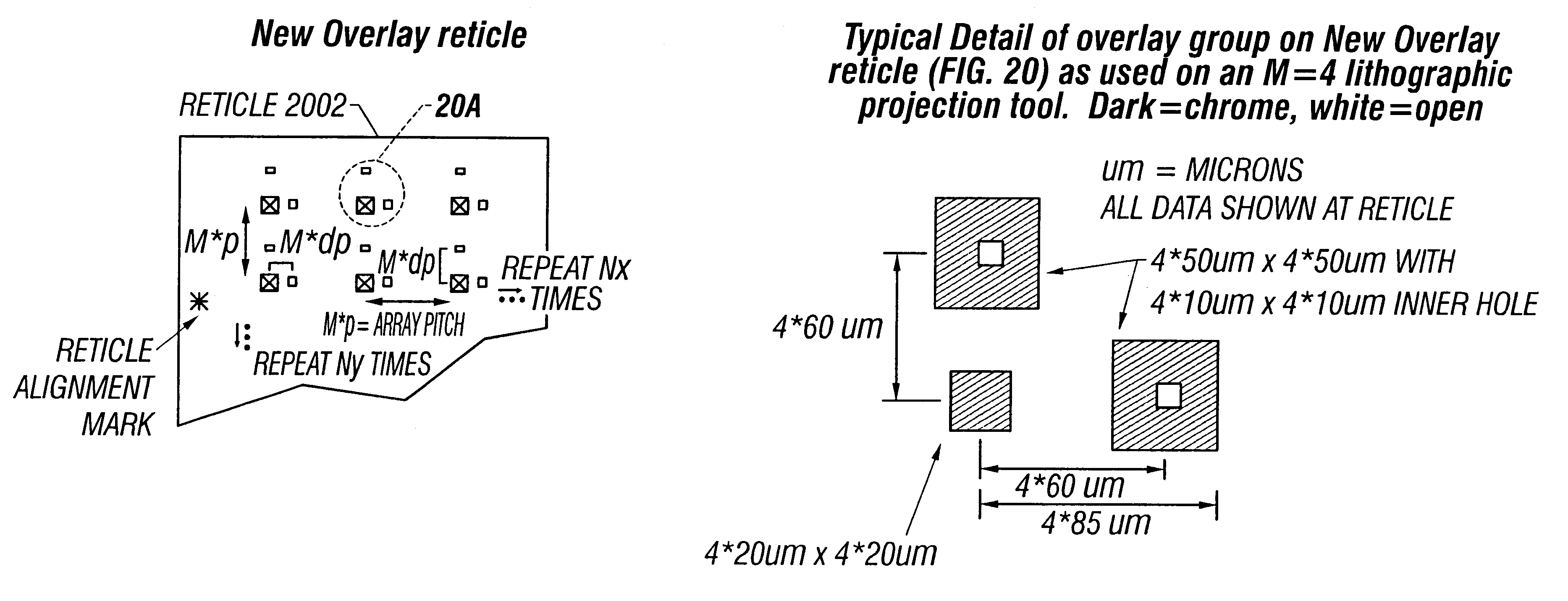
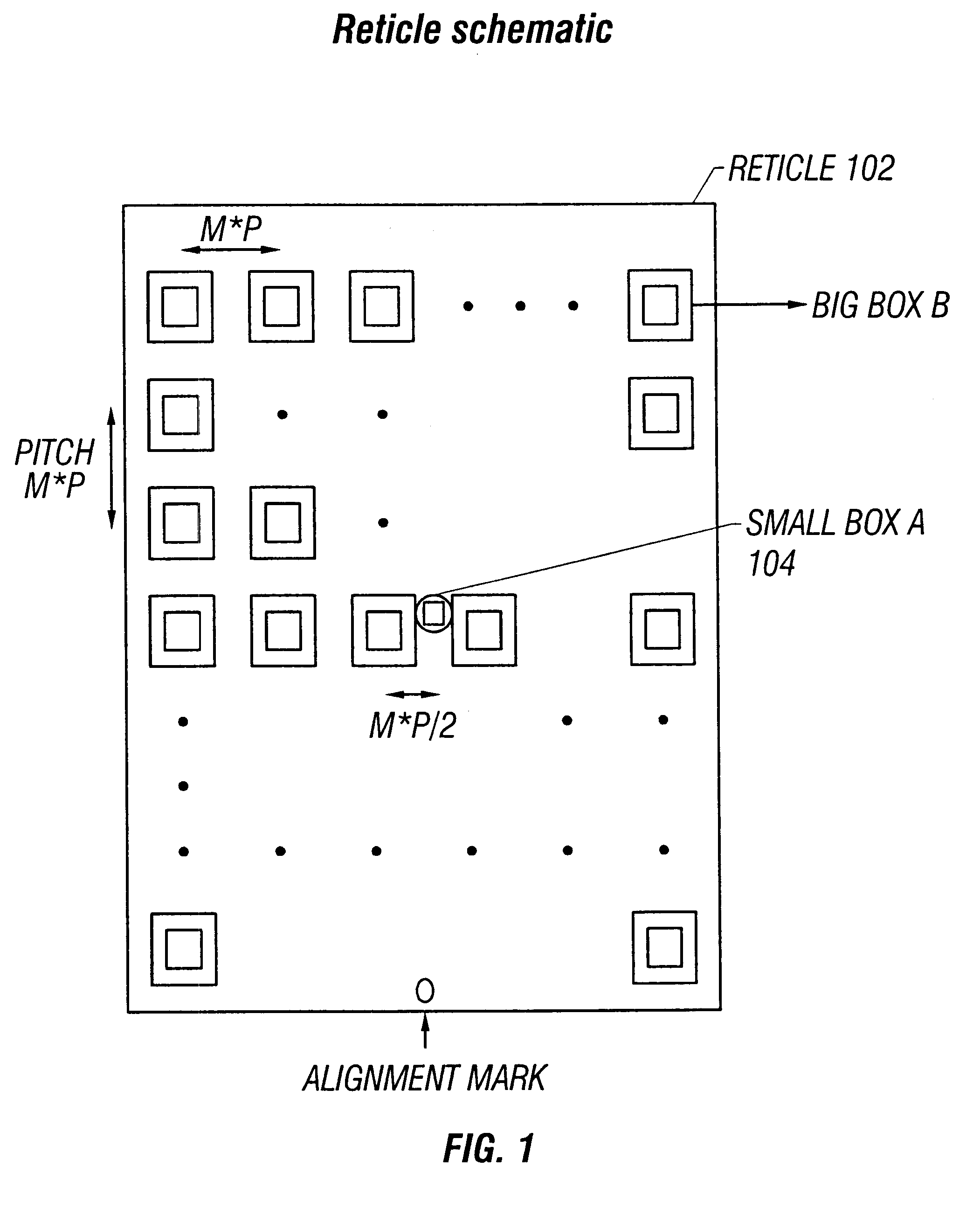
Yet another embodiment allows for the extraction of lens distortion placement error excluding total translation, rotation, and overall scale or magnification overlay error and is mathematically decoupled from stage error. FIG. 15 illustrates this embodiment in terms of a process flow diagram. First in block 1502, a wafer is provided. Typically it already has alignment marks suitable for use at normal orientation (0 degrees) and when rotated by 90-degrees as shown in FIG. 22. In cases where the projection imaging tool, or machine, is capable of realigning an unpatterned wafer after a 90-degree rotation to 120%*max(Lx, Ly), where the exposure field has rectangular dimension Lx.times.Ly. Each full-field exposure produces an Mx.times.My array (Mx<=Nx, My<=Ny) of overlay groups at the wafer surface shown by the solid line overlay groups of FIGS. 11, 12, 25.

Using the same reticle the wafer stage is blind stepped to expose the second layer of the X-shear pattern with field center located a...


PUM

PropertyMeasurementUnit
rotationaaaaaaaaaa
distanceaaaaaaaaaa
semiconductoraaaaaaaaaa

Abstract

A projection lens distortion error map is created using standard overlay targets and a special numerical algorithm. A reticle including a 2-dimensional array of standard overlay targets is exposed several times onto a photoresist coated silicon wafer using a photolithographic stepper. After exposure, the overlay targets are measured for placement error using a conventional overlay metrology tool. The resulting overlay error data is then supplied to a software program that generates a lens distortion error map for the photolithographic projection system.

Description

1. Field of the InventionThe present invention relates generally to optical metrology and more particularly to characterizing and monitoring the intra-field distortions of projection imaging systems used in semiconductor manufacturing.2. Description of the Related ArtToday's lithographic processing requires ever tighter layer-to-layer overlay tolerances to meet device performance requirements. Overlay registration is defined as the translational error that exists between features exposed layer to layer in the vertical fabrication process of semiconductor devices on silicon wafers. Other names for overlay registration include, registration error and pattern placement error, and overlay error. Overlay registration on critical layers can directly impact device performance, yield and repeatability. Increasing device densities, decreasing device feature sizes and greater overall device size conspire to make pattern overlay one of the most important performance issues during the semicondu...

Claims


Application Information

Patent Timeline
Patent Type & Authority Patents(United States)
IPC IPC(8): G03F7/20
CPCG03F7/70558G03F7/70633G03F7/706Y10S977/887
Inventor SMITH, ADLAIMCARTHUR, BRUCEHUNTER, JR., ROBERT
Owner LITEL INSTR
Why Eureka
Try Eureka