Small-angle scattering x-ray metrology systems and methods

a technology of x-ray metrology and small-angle scattering, applied in the field of semiconductor metrology, can solve the problems of final device not meeting the desired performance, final device malfunction, adversely affecting yield,

Active Publication Date: 2015-04-23
KLA CORP
View PDF3 Cites 119 Cited by
  • Summary
  • Abstract
  • Description
  • Claims
  • Application Information

AI Technical Summary

Problems solved by technology

These variations, if uncorrected, can cause the final device to fail to meet the desired performance due to electrical timing errors.
Even worse, these errors can cause final devices to malfunction and adversely affect yield.
This technique is time consuming (e.g., several hours).
Additionally, buried defects can be difficult to detect with certain metrology tools.
Although these techniques can help verify the existence of voids, the sample is destroyed during the analysis.
This technique is expensive for integrated circuit manufacturers since it means sacrificing product samples from the product line and often results in wasting product found to have no significant defects.
Furthermore, FIB techniques are time consuming, which can cause downtime of the product line production.
This increased downtime can be an especially big problem if numerous scans on numerous wafers are needed to ensure void-free processing.

Method used


Image

  • Small-angle scattering x-ray metrology systems and methods
  • Small-angle scattering x-ray metrology systems and methods
  • Small-angle scattering x-ray metrology systems and methods

Examples


Embodiment Construction

[0028]In the following description, numerous specific details are set forth in order to provide a thorough understanding of the present invention. The present invention may be practiced without some or all of these specific details. In other instances, well known process operations have not been described in detail to not unnecessarily obscure the present invention. While the invention will be described in conjunction with the specific embodiments, it will be understood that it is not intended to limit the invention to the embodiments.

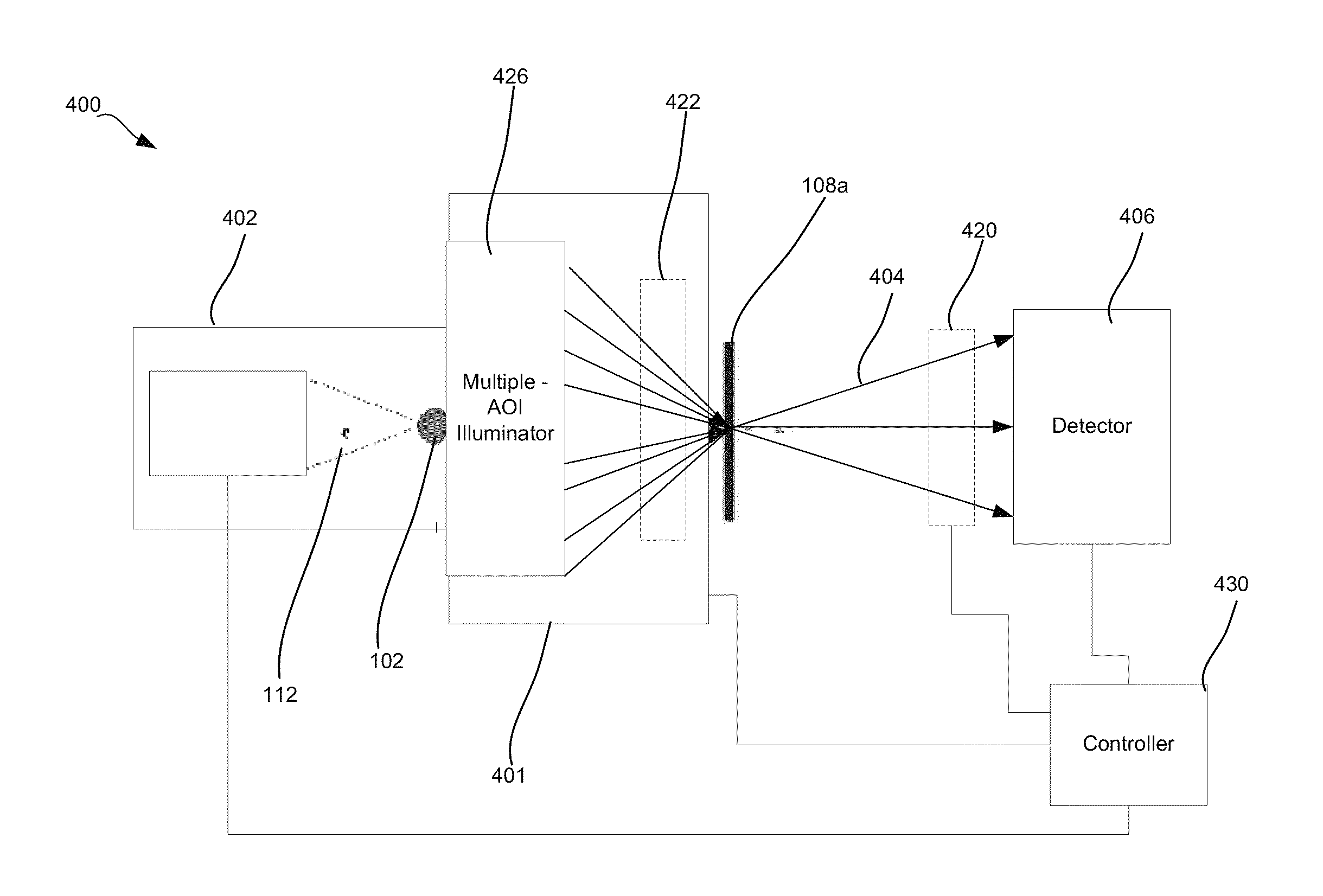
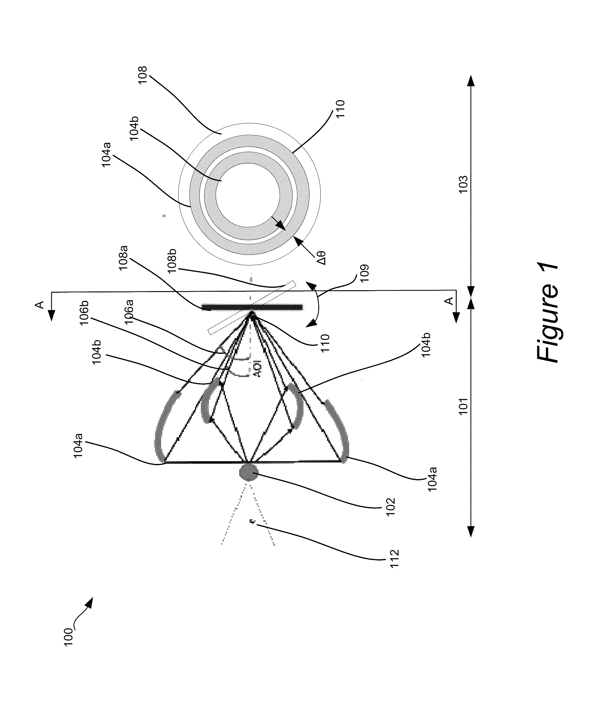
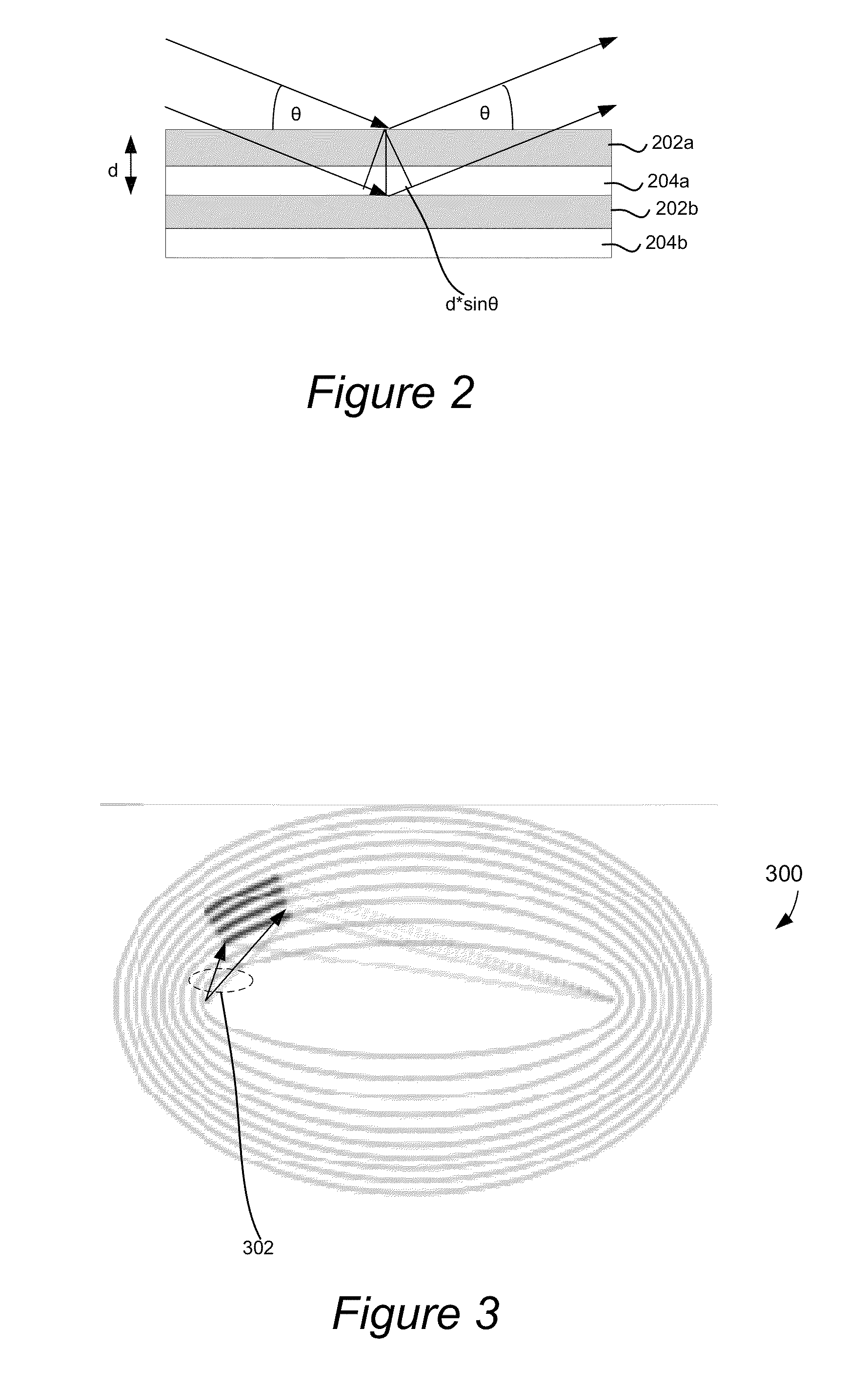
[0029]Certain embodiments of the present invention provide a scatterometry apparatus with small angle x-ray scattering (SAXS) capabilities. This system may include a high brightness x-ray source coupled with a high efficiency x-ray illumination system with improved measurement capabilities. A SAXS system is capable of measuring geometric parameters in semiconductor structures such as overlay, pitch, critical dimensions (CD), height, side wall angle (SW...


PUM

PropertyMeasurementUnit
line-edge roughnessaaaaaaaaaa
thicknessaaaaaaaaaa
energyaaaaaaaaaa

Abstract

Disclosed are apparatus and methods for performing small angle x-ray scattering metrology. This system includes an x-ray source for generating x-rays and illumination optics for collecting and reflecting or refracting a portion of the generated x-rays towards a particular focus point on a semiconductor sample in the form of a plurality of incident beams at a plurality of different angles of incidence (AOIs). The system further includes a sensor for collecting output x-ray beams that are scattered from the sample in response to the incident beams on the sample at the different AOIs and a controller configured for controlling operation of the x-ray source and illumination optics and receiving the output x-rays beams and generating an image from such output x-rays.

Description

CROSS-REFERENCE TO RELATED APPLICATIONS[0001]This application claims the benefit of prior application U.S. Provisional Application No. 61 / 893,341, filed 21 Oct. 2013 by Michael S. Bakeman et al., which application is herein incorporated by reference in its entirety for all purposes.TECHNICAL FIELD OF THE INVENTION[0002]The present invention relates generally to methods and systems for semiconductor metrology and, more specifically, to using x-ray illumination.BACKGROUND[0003]Photolithography or optical lithography systems used in the manufacture of integrated circuits have been around for some time. Such systems have proven extremely effective in the precise manufacturing and formation of very small details in the product. In some photolithography systems, a circuit image is written on a substrate by transferring a pattern via a light or radiation beam (e.g., UV or ultraviolet light). For example, the lithography system may include a light or radiation source that projects a circuit...

Claims


Application Information

Patent Timeline
Patent Type & Authority Applications(United States)
IPC IPC(8): G01N23/201G01N33/00
CPCG01N23/201G01N2033/0095G01N33/00G01N23/207
Inventor BAKEMAN, MICHAEL S.SHCHEGROV, ANDREI V.LEVY, ADYZHUANG, GUORONG V.HENCH, JOHN J.
Owner KLA CORP
Why Eureka
Try Eureka