Method for making monolithic patterned dichroic filter detector arrays for spectroscopic imaging

a detector array and dichroic filter technology, applied in the field of making an improved detector array, can solve the problems of weakening the walls formed by the photoresist, the art of microlithography has been limited to the field of microelectronics, and the filter art has not produced thin filters with well-defined edges, etc., and achieves the effect of weakening the walls

Inactive Publication Date: 2003-10-28
OCEAN OPTICS
View PDF3 Cites 63 Cited by
  • Summary
  • Abstract
  • Description
  • Claims
  • Application Information

AI Technical Summary

Problems solved by technology

As mentioned earlier, the optical arts have failed to produce thin filters having well-defined edges, and the art of microlithography has been limited to the field of microelectronics.
Photoresist is applied to the wafer prior exposure and over development to create an undercut, thereby weakening the walls formed by the photoresist.

Method used


Image

  • Method for making monolithic patterned dichroic filter detector arrays for spectroscopic imaging
  • Method for making monolithic patterned dichroic filter detector arrays for spectroscopic imaging
  • Method for making monolithic patterned dichroic filter detector arrays for spectroscopic imaging

Examples


Embodiment Construction

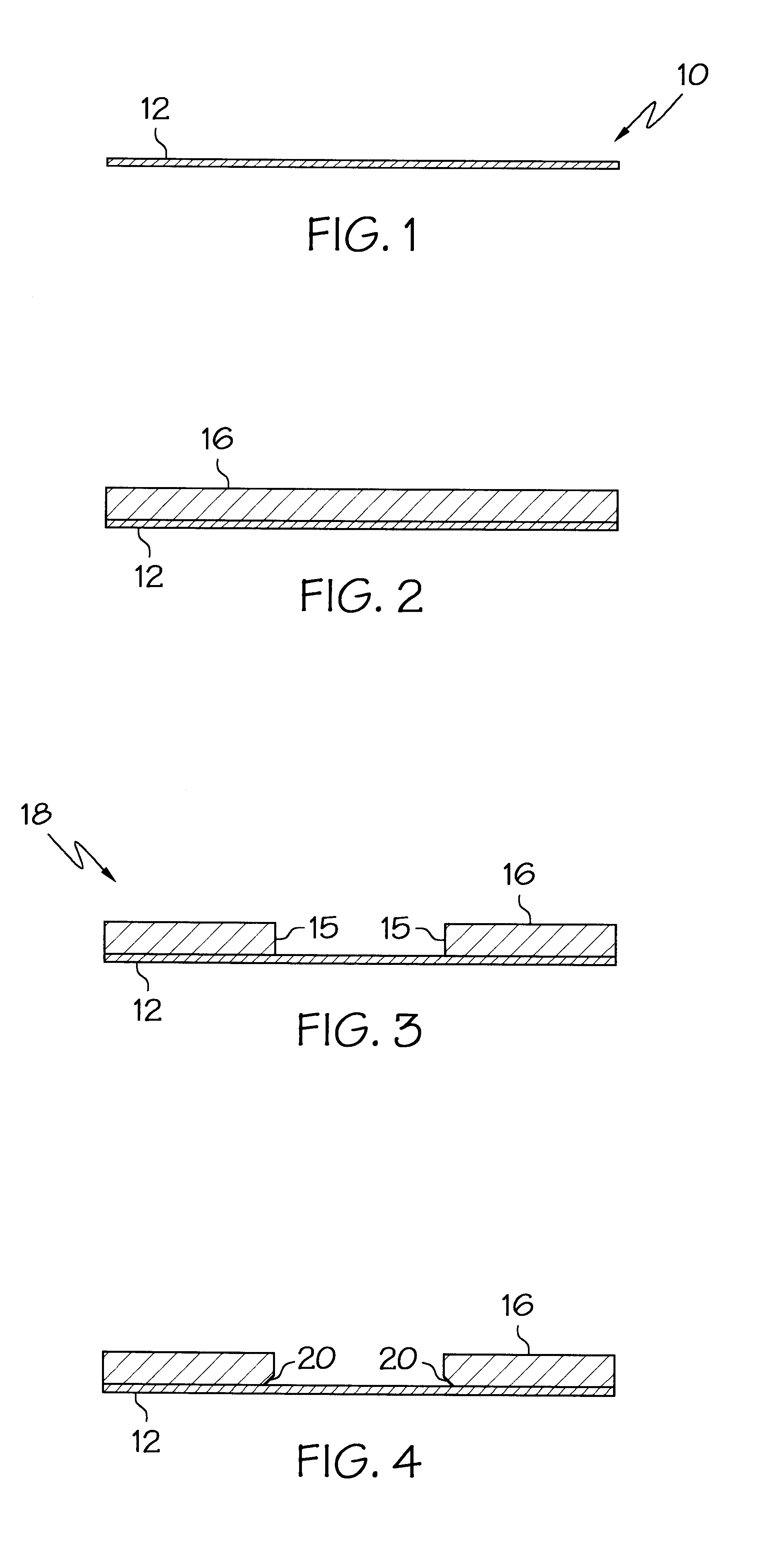
Referring now to FIG. 1, it will there be seen that the first step in an exemplary embodiment of that includes cleaning and preparing a wafer 12 by conventional means. Rouge and acetone are typically employed in a well-known way resulting in the prepared wafer 12 shown in FIG. 1 and is denoted 10 as a whole.

A suitable photoresist, such as Shipley PR1818, for example, is then applied. In FIG. 2, which depicts the second step of the novel process, the photoresist is denoted by the reference numeral 16; it is about 0.8-2.5 microns in thickness. Photoresist layer 16 is applied by a conventional spin technique, well known in the art, and is then baked to remove solvents therefrom in the well-known way.

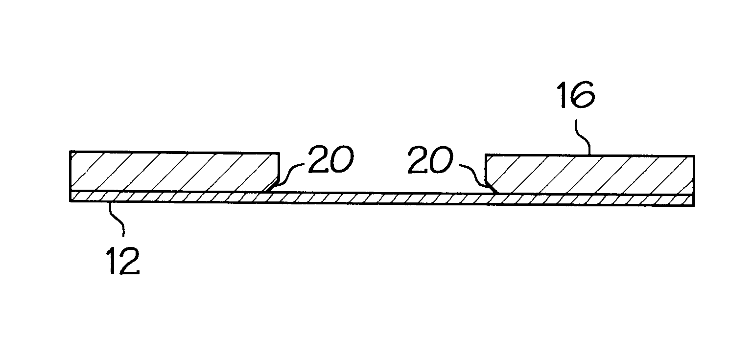
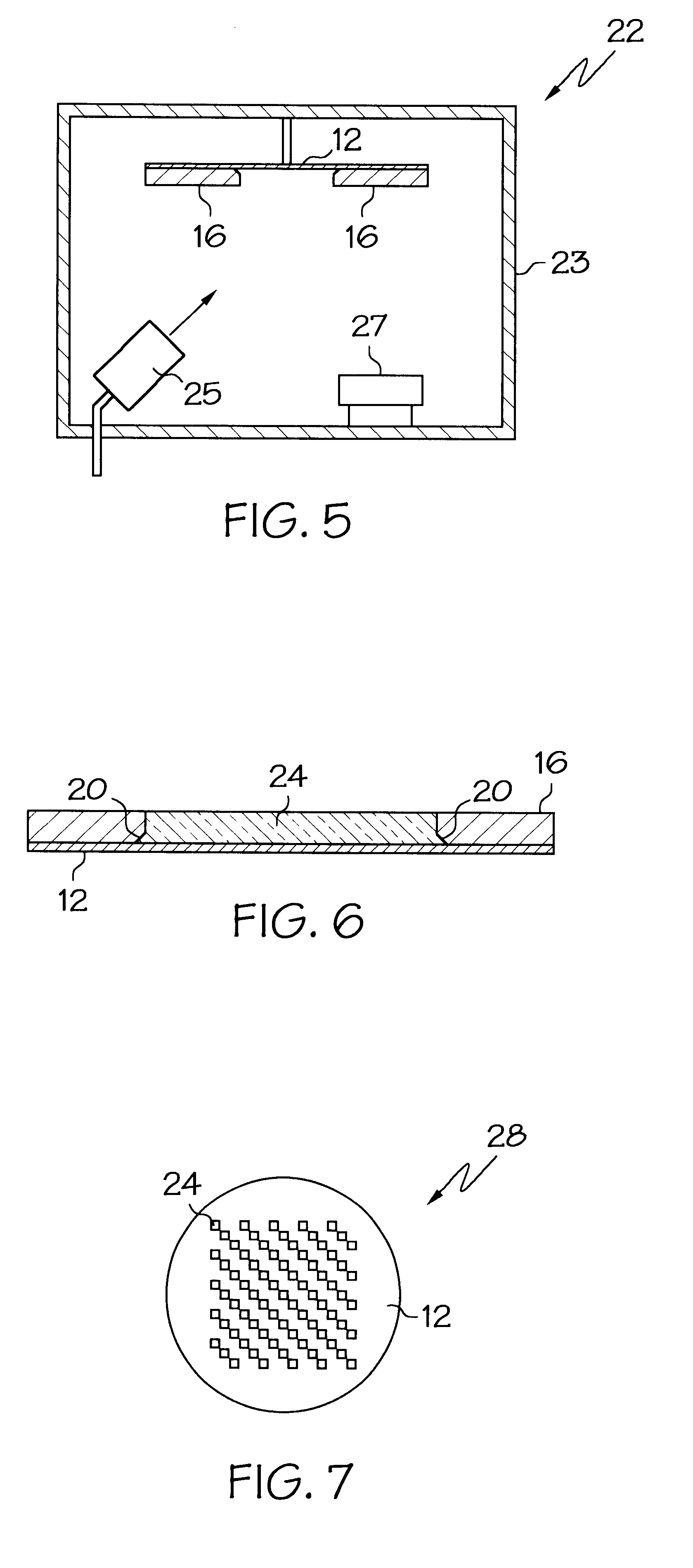
The assembly is then contact or proximity printed to a mask for one of the three primary colors in the case of dichroic filters for color measurement, or one of several filters representing a set of coefficients in the spectral model. For chemical sensing the unmasked part of the photoresis...


PUM

PropertyMeasurementUnit
thicknessaaaaaaaaaa
widthaaaaaaaaaa
included angleaaaaaaaaaa

Abstract

A monolithic patterned dichroic filter array is mounted on a wafer by combining microelectronic and microlithography techniques. A wafer is coated with a photoresist. The assembly is masked, and the unmasked photoresist, after exposure to ultraviolet light, is developed to expose a predetermined section. That section of wafer is then over developed to create an undercut in its walls and to expose the underlying wafer. Dichroic filter material is then deposited onto the wafer by a cold process, and the photoresist layer is then removed, leaving only the dichroic filter material on the wafer. The process is repeated to create an array. The finished wafer is then bonded to a linear or two dimensional detector array, or to a glass window that is then bonded to a linear or two dimensional detector, to create a high performance spectral detector for spectroscopic imaging. When placed on a two dimensional detector in a camera, an imaging system capable of showing spatial variation in color, chemicals or other spectrally dependent parameters is produced.

Description

FIELD OF THE INVENTIONThis invention relates, generally, to methods for making an improved detector array and more specifically a method for making a monolithic patterned dichroic filter detector array for spectroscopic imaging by coupling a patterned dichroic filter to a linear or two dimensional detector array such as a Charge Coupled Device, and the like.BACKGROUND OF THE INVENTIONColor-dyed gels positioned in front of detector arrays are currently employed to produce spectral detectors. The gels have a number of shortcomings, however, that limit their utility. For example, they do not function over a wide temperature range and thus cannot meet strict specifications of the type that might be called for in military applications, for example. Moreover, gels absorb relatively high levels of light and thus require more power to produce a desired detection level than would a less absorptive material. Moreover, the colors of the gels are not easily controlled during their manufacture, ...

Claims


Application Information

Patent Timeline
Patent Type & Authority Patents(United States)
IPC IPC(8): G02B5/20
CPCG02B5/20G01J3/02G02B5/201H01L31/02162H01L27/14685
Inventor BUCHSBAUM, PHILIP E.MORRIS, MICHAEL J.
Owner OCEAN OPTICS
Why Eureka
Try Eureka