Electro-optical device and electronic apparatus

a technology of optical devices and electronic devices, applied in the direction of static indicating devices, lighting and heating devices, instruments, etc., can solve the problems of ineffective use of light sources, inability to use light, and disadvantages of large-scale light sources having high directivity

Inactive Publication Date: 2003-11-04
138 EAST LCD ADVANCEMENTS LTD
View PDF8 Cites 68 Cited by
  • Summary
  • Abstract
  • Description
  • Claims
  • Application Information

AI Technical Summary

Problems solved by technology

It is very disadvantageous to use a large-scale light source having high directivity as a light source of a display device (electro-optical device) of such electronic apparatuses.
Thus, such a light source is not actually used.
However, related art display devices have the following problems.
Light which has returned after being emitted from the light source and reflected at the portion that does not pass light is absorbed by any one of the members, so that the light cannot be used.
For this reason, the efficiency with which the light from the light source is used is low.
Therefore, even if a micro-lens array is used, the light from the light source cannot be efficiently gathered at a light-transmissive window of the liquid crystal panel.
In this way, in related art display devices (electro-optical devices), light from the light source cannot be efficiently gathered at the light-transmissive window, so that the efficiency with which the light emitted from the light source is used is low.

Method used


Image

  • Electro-optical device and electronic apparatus
  • Electro-optical device and electronic apparatus
  • Electro-optical device and electronic apparatus

Examples


first embodiment

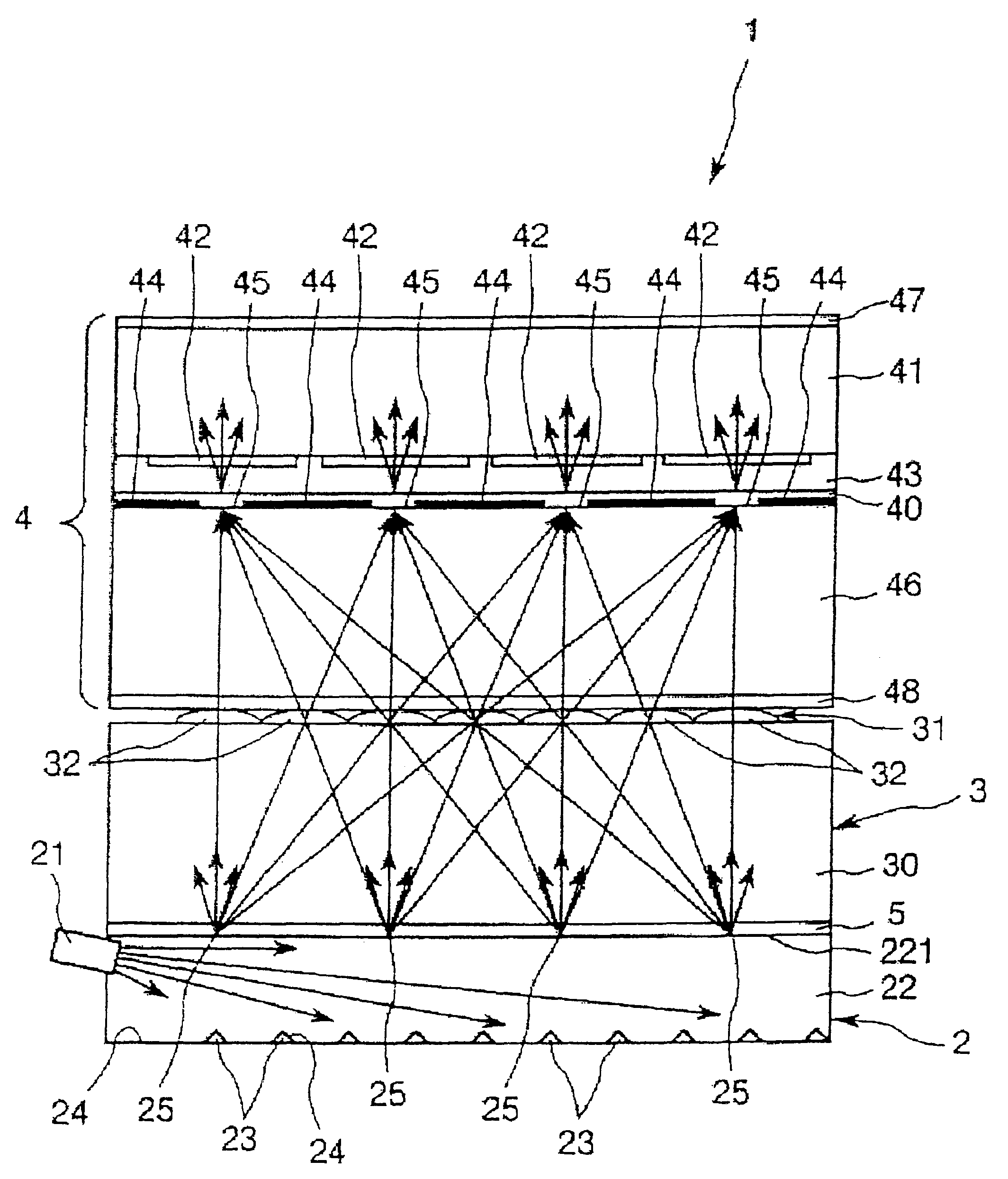
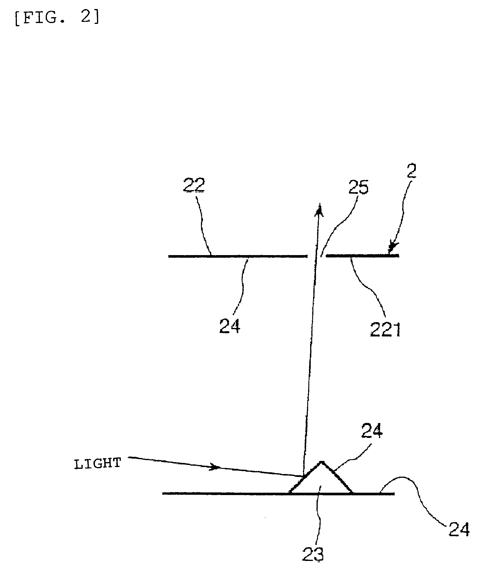
FIG. 1 is a vertical sectional view schematically showing the structure of an electro-optical device in accordance with the present invention. For simplification, slanting lines indicating a cross section are not shown in FIG. 1. In addition, for simplification, only the primary optic axis of light that passes the center of micro-lenses 32 is shown in FIG. 1.

A display device (electro-optical device) 1, shown in FIG. 1, is a transflective display device, and includes a light source device 2, which is a backlight, a micro-lens array plate 3, and a transflective liquid crystal panel (light modulation device) 4 including a plurality of light-transmissive windows.

The light source device 2 is positioned at the lower side in FIG. 1; the liquid crystal panel 4 is positioned at the upper side in FIG. 1; and the micro-lens array plate 3 is positioned between the light source device 2 and the liquid crystal panel 4.

The light source device 2 and the micro-lens array plate 3 are adhered (joined)...

second embodiment

A description of an electro-optical device of the present invention will now be provided.

FIG. 7 is a vertical sectional view schematically showing the structure of the second embodiment of the electro-optical device of the present invention. For simplification, slanting lines indicating a cross section are not shown in FIG. 7. In addition, for simplification, only the primary optic axis of light that passes the center of micro-lenses 32 is shown in FIG. 7.

Hereunder, the description of a display device (electro-optical device) 1 of the second embodiment will be centered on the differences between it and the display device 1 of the first embodiment, so that similar features will not be discussed in the description.

The display device 1, shown in FIG. 7, is a transmissive display device and includes a transmissive liquid crystal panel 4a in place of the transflective liquid crystal panel 4 of the display device 1 of the above-described first embodiment. The other structural features are...

third embodiment

Next, a description of an electro-optical device of the present invention will be provided.

FIG. 8 is a vertical sectional view schematically showing the structure of the third embodiment of the electro-optical device of the present invention. For simplification, slanting lines indicating a cross section are not shown in FIG. 8. In addition, for simplification, only the primary optic axis of light that passes the center of micro-lenses 32 is shown in FIG. 8.

Hereunder, the description of a display device (electro-optical device) 1 of the third embodiment will be centered on the differences between it and the display device 1 of the first embodiment, so that similar features will not be discussed in the description.

Although a display device 1, shown in FIG. 8, is a transflective display device including a transflective liquid crystal panel (light modulation device) 4, it may be a transmissive display device including a transmissive liquid crystal panel (light modulation device) 4a like...


PUM

PropertyMeasurementUnit
refractive indexaaaaaaaaaa
optical distanceaaaaaaaaaa
optical distance Laaaaaaaaaaa

Abstract

An electro-optical device which includes a plurality of point light sources, a micro-lens array in which a plurality of micro-lenses are disposed, and a light modulation device including a plurality of light-transmissive windows. The electro-optical device is constructed so that, by the micro-lens array, light from the plurality of point light sources is focused at the light-transmissive windows.

Description

1. Field of InventionThe present invention relates to an electro-optical device and an electronic apparatus using the electro-optical device.2. Description of Related ArtThere is a demand that electronic apparatuses, such as personal computers and portable devices, be smaller and thinner. It is very disadvantageous to use a large-scale light source having high directivity as a light source of a display device (electro-optical device) of such electronic apparatuses. Thus, such a light source is not actually used.Therefore, for example, in a liquid crystal display device, a method is used in which light from a light source is guided to the back surface of a liquid crystal panel by a light guide member in order to illuminate the liquid crystal panel from the back surface thereof using, for example, a reflector plate, a diffusing plate, or a prism sheet.However, related art display devices have the following problems.For example, when the display device includes a transmissive liquid cr...

Claims


Application Information

Patent Timeline
Patent Type & Authority Patents(United States)
IPC IPC(8): G02F1/1335G02B3/00G02F1/13G02B5/04
CPCG02F1/133555G02F1/133526G02B5/045G02B3/0006G02F1/1335
Inventor MIYAMAE, AKIRANAGASAKA, KIMIOOKUMURA, OSAMU
Owner 138 EAST LCD ADVANCEMENTS LTD
Why Eureka
Try Eureka