Method for active wafer centering using a single sensor

a single sensor and active technology, applied in the field of position control or centering, can solve the problems of cheng design and loss of wafers, and achieve the effect of improving the accuracy of the wafer processing system and improving the accuracy of the wafer

Inactive Publication Date: 2004-07-13
NOVELLUS SYSTEMS
View PDF10 Cites 63 Cited by
  • Summary
  • Abstract
  • Description
  • Claims
  • Application Information

AI Technical Summary

Problems solved by technology

As wafers transfer from station to station in a semiconductor manufacturing system, tolerance stack-up as well as handling problems, such as ESC sticking, result in wafer offset that causes process shift, which may ultimately lead to wafer loss.
This makes the Cheng design ill suited to multiple chamber wafer processing systems.

Method used


Image

  • Method for active wafer centering using a single sensor
  • Method for active wafer centering using a single sensor
  • Method for active wafer centering using a single sensor

Examples


Embodiment Construction

)

In describing the preferred embodiment of the present invention, reference will be made herein to FIGS. 1-2 of the drawings in which like numerals refer to like features of the invention.

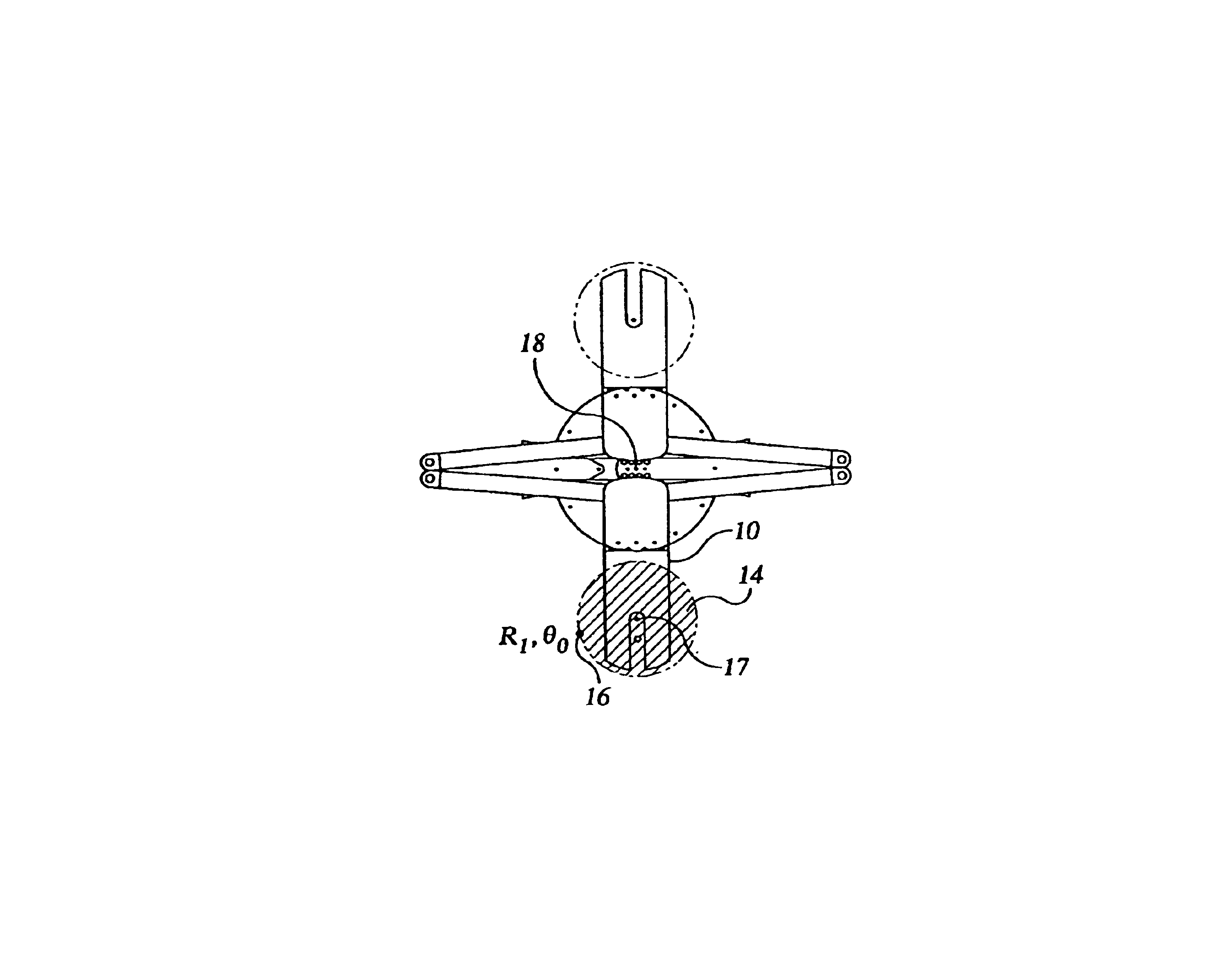
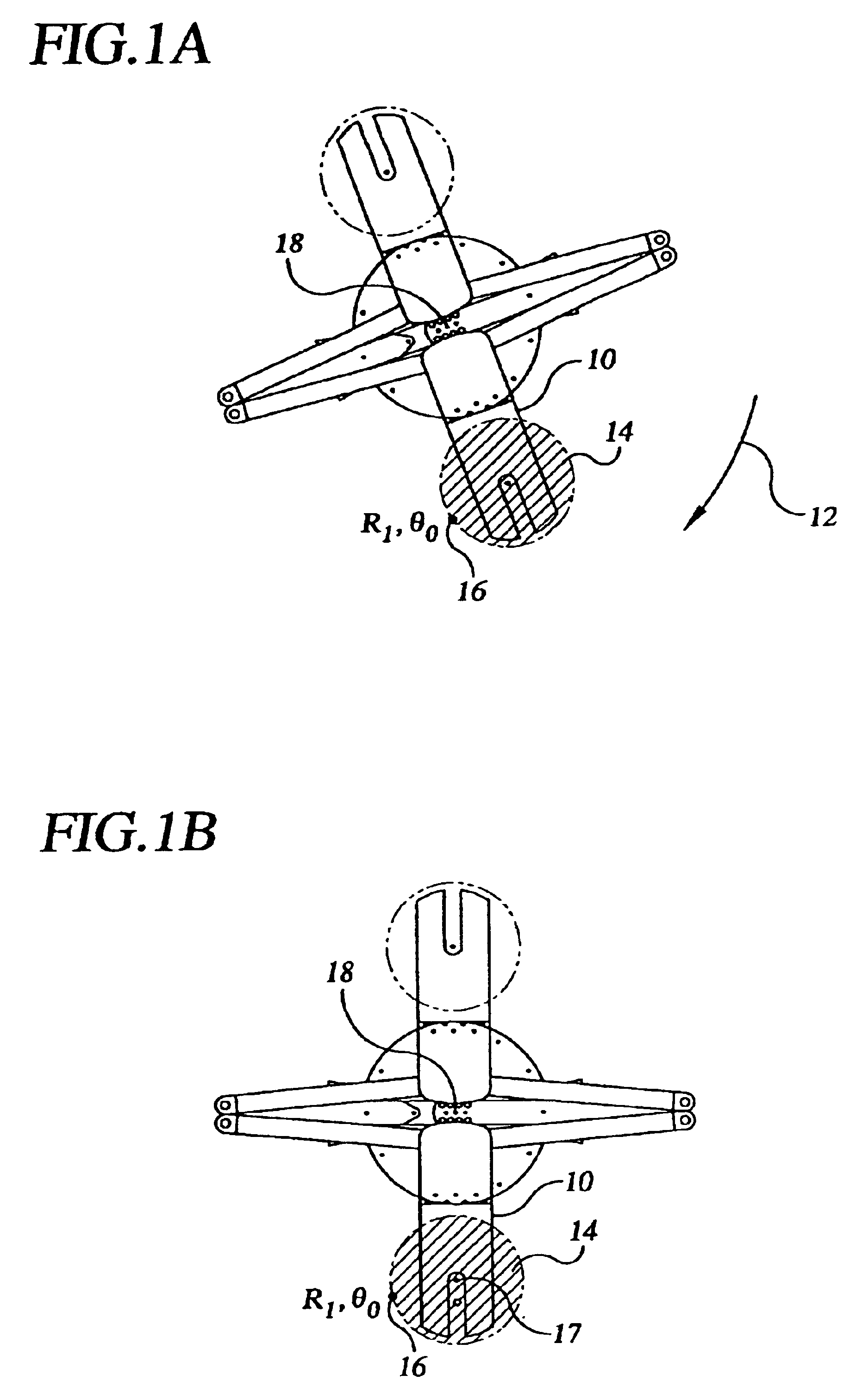
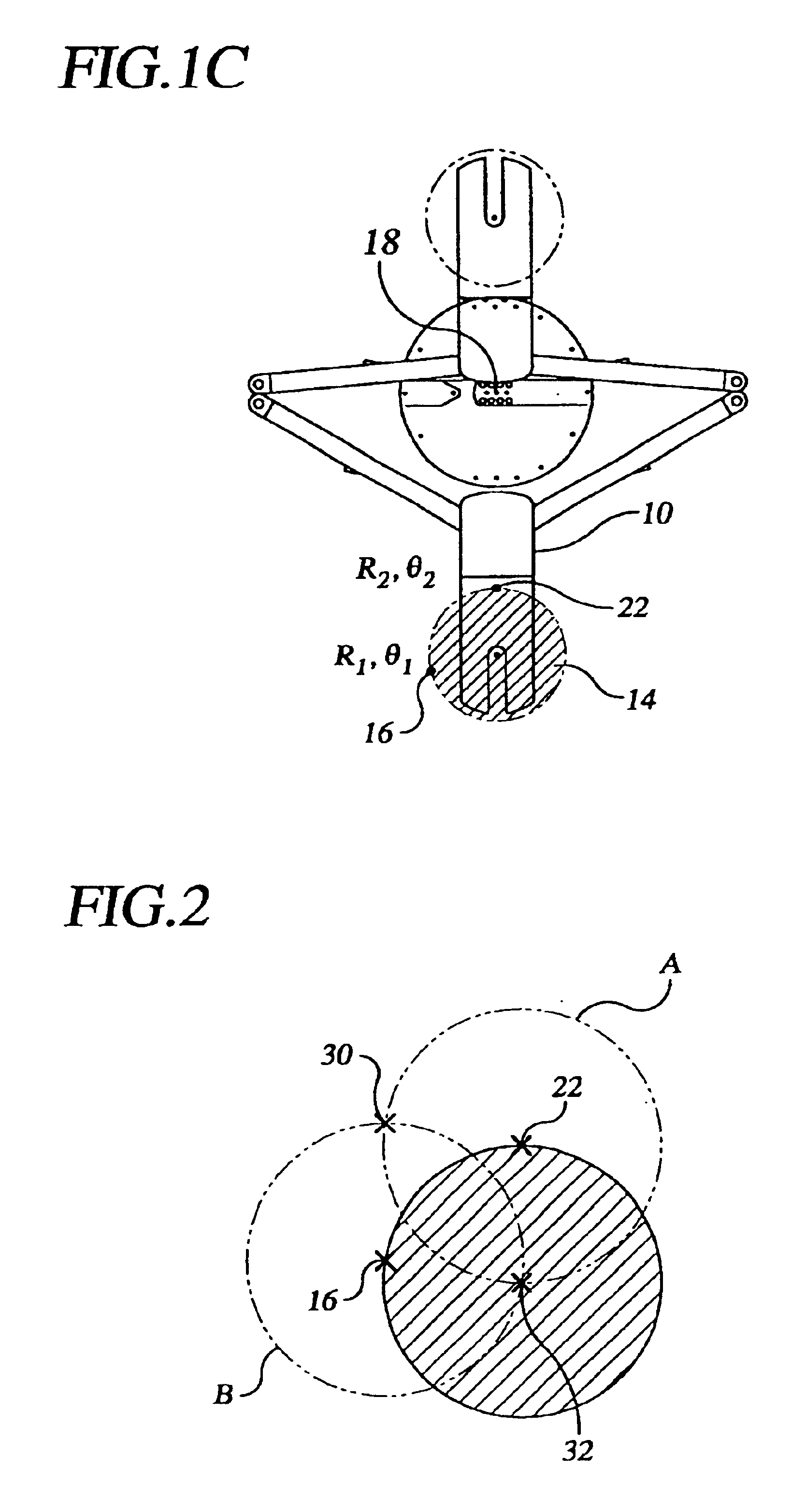
The process described herein allows a robotic apparatus to correct for wafers that have become offset or off-center during wafer processing. This is accomplished by determining the amount of offset and re-centering the wafer during wafer transport to the next process station using a single station sensor to locate the wafer center point.

The apparatus for conducting the preferred method of wafer centering includes primarily a semiconductor wafer handling sub-system that is comprised of a chamber, a robotic arm for transferring wafers to a plurality of stations with at least one sensor located at a point in front of each station. The method of operation employs the single sensors located at each station to acquire directional coordinates for designated points on the wafer's edge. This gives the insta...


PUM


Abstract

A method for a robotic semiconductor wafer processing system to correct for wafers that have become offset or off-center during wafer processing. This is accomplished by determining the amount of offset and re-centering the wafer during wafer transport to the next process station using a single station sensor to locate the wafer center point. Each single sensor located at each station activates when the wafer's edge traverses through the sensor's path. Directional coordinates for the measured designated points on the wafer's edge are calculated, and the intersection points of two circles, analytically derived from using the measured designated points as their centers, are determined. The intersection point closest to the true wafer center position represents the measured wafer's center point. This point is compared to the true wafer center position, and the wafer is then adjusted for this difference.

Description

1. Field of the InventionThe invention relates to semiconductor wafer processing, and more specifically, to position control or centering of a wafer on the semiconductor manufacturing tool's robotic arm, for positioning and repositioning of the wafer during wafer transport.2. Description of Related ArtAs wafers transfer from station to station in a semiconductor manufacturing system, tolerance stack-up as well as handling problems, such as ESC sticking, result in wafer offset that causes process shift, which may ultimately lead to wafer loss. It is therefore desirable for the transfer robot to measure wafer offset and correct this offset at each station transfer.Typically, multiple sensors are required to empirically and analytically derive the wafer center position. Sensors can be activated upon wafer movement, and a plurality of sensors can be used to determine the wafer's exact position in a station at a given moment. In U.S. Pat. No. 5,483,138 issued to Shmookler et al. on Jan. ...

Claims


Application Information

Patent Timeline
Patent Type & Authority Patents(United States)
IPC IPC(8): H01L21/00
CPCH01L21/67265Y10S414/136
Inventor MARTINSON, ROBERTSHRIVASTAVA, DHAIRYAWEIS, MATTHEW
Owner NOVELLUS SYSTEMS
Why Eureka
Try Eureka