Method of manufacturing multi-chip stacking package

a technology of stacking package and manufacturing method, which is applied in the direction of manufacturing tools, printed circuit manufacturing, and semiconductor/solid-state device details, etc., can solve the problems of easy rise of wire sway and short circui

Inactive Publication Date: 2004-11-23
ADVANCED SEMICON ENG INC
View PDF9 Cites 25 Cited by
  • Summary
  • Abstract
  • Description
  • Claims
  • Application Information

AI Technical Summary

Problems solved by technology

The drawback of the package 10 in FIG. 1 is that the wire span of the metal bonding wire 14 is so long due to the connection from the wire bonding pad 17 of the second chip 12 to the bonding pad 18 of the substrate 15, such that a wire sway problem will rise easily and causes a short circuit during the process of encapsulation.
However, in that prior patent specification, how to complete the flip-chip bonding for the two chips was not disclosed explicitly, and the structural characteristic of the combination part of the two chips was not presented in detail, either.
Furthermore, one of the at least two chips may only provide a bonding pad similar to the Under Bump Metallurgy 43 and may not provide with bumps, and using the bonding pad to be welded with the bump on another chip.

Method used


Image

  • Method of manufacturing multi-chip stacking package
  • Method of manufacturing multi-chip stacking package
  • Method of manufacturing multi-chip stacking package

Examples


Embodiment Construction

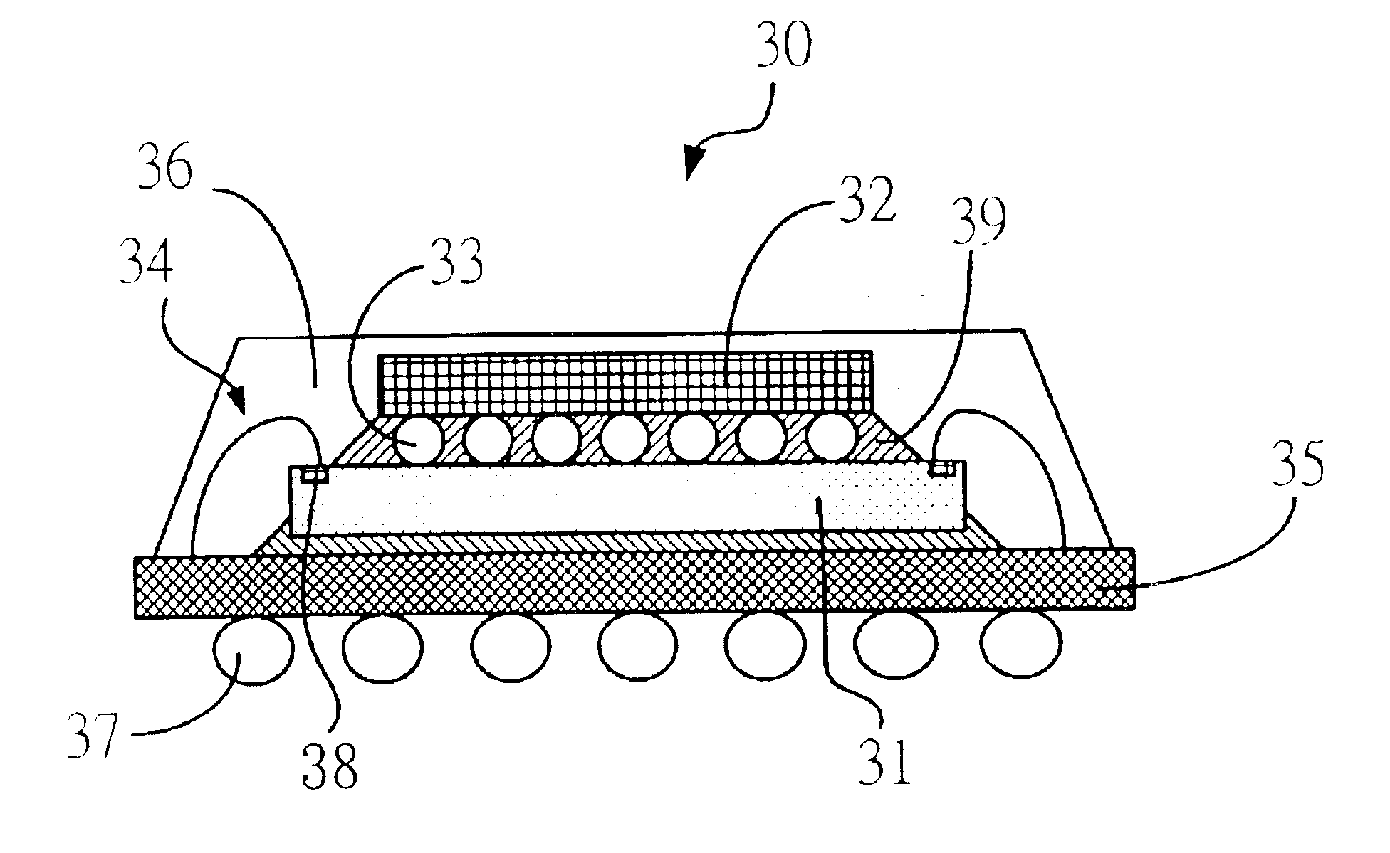
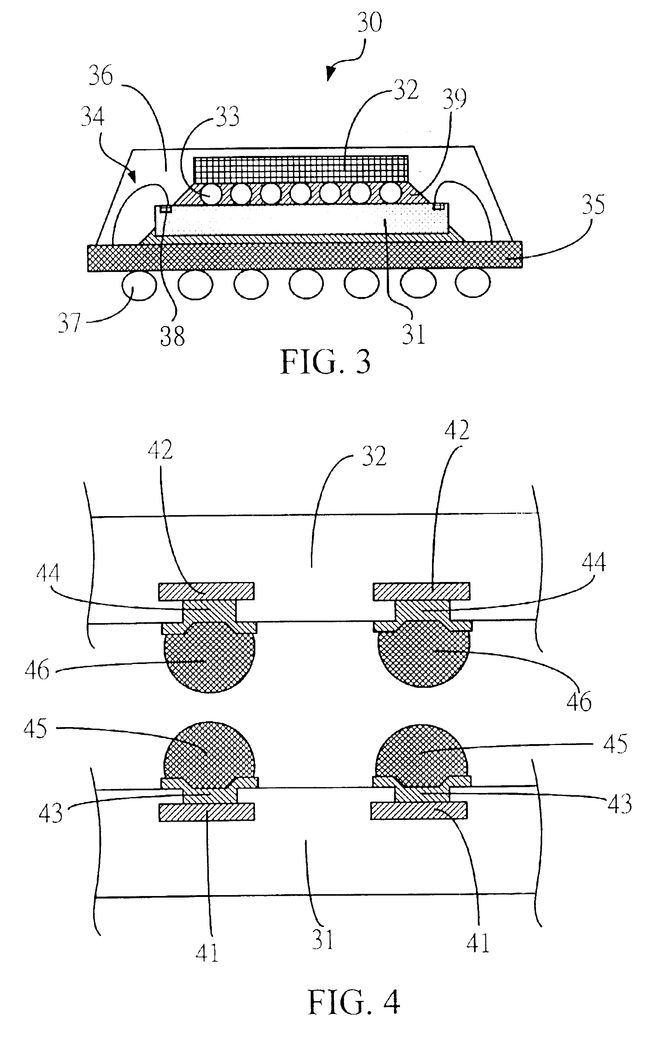
FIG. 3 shows a schematic view of the multi-chip stack package 30 according to one preferred embodiment of the invention. The multi-chip stack package 30 includes a first chip 31, a second chip 32, a substrate 35 and a plurality of solder balls 37. The first chip 31 and second chip 32 are bonded by welded bumps 33 via flip-chip bonding, and the first chip 31 is attached to / onto the upper surface of the substrate 35 with adhesive. A plurality of wire bonding pads 38 are configured on the periphery of the active surface of the first chip 31 and are not covered by the underfill 39 surrounding the welded bump. The wire bonding pads 38 can achieve the electrical signal connection via the metal bonding wires 34 and the substrate 35. The multi-chip stacking structure on the upper surface of the substrate 35 is protected by the covering of the encapsulant 36, and the lower surface of the substrate 35 provides a plurality of solder balls 37 as electrical contacts with the circuit board (not s...


PUM

PropertyMeasurementUnit
pressureaaaaaaaaaa
areaaaaaaaaaaa
thicknessaaaaaaaaaa

Abstract

The present invention discloses a method of manufacturing a multi-chip stacking package. The characteristic of the invention is that after the alignment of the bumps of at least two chips, welded bumps will be generated in a high temperature welding to form a welded bump. Furthermore, one of the at least two chips may only provide bonding pad similar to the Under Bump Metallurgy and may not provide bumps, and using the bonding pad to be welded with the bump on another chip.

Description

1. Field of the InventionThe invention relates to a method of manufacturing a multi-chip stacking package, especially to a method of manufacturing multi-chip package using flip-chip bonding to complete the chip stacking.2. Background of the InventionToward the increasing requirements for portability of electronic consumer products, undoubtedly the multi-chip module packaging technology is the best way to meet such requirements. However, the technologies for integrating the functions of many chips and reducing the area occupied by the package mostly need to stack the chips into a packaging device of 3-D structure.FIG. 1 shows a cross-sectional schematic view of a conventional multi-chip stacking package 10, which is disclosed in the specification of Taiwan Patent Publication No. 444,364. The package 10 is characterized in that the active surface of the first chip 11 is welded to the upper surface of the substrate 15 with a plurality of bumps 13. Furthermore, the passive surface of a ...

Claims


Application Information

Patent Timeline
Patent Type & Authority Patents(United States)
IPC IPC(8): H01L21/70H01L21/98H05K13/00
CPCH01L25/50Y10T29/49169H01L2224/16225H01L2224/32145H01L2224/32245H01L2224/48091H01L2224/48227H01L2224/48247H01L2224/73204H01L2224/73265H01L2924/01079H01L2924/15311H01L2224/16145Y10T29/49117Y10T29/49144Y10T29/49149Y10T29/4913H01L2224/32225H01L2924/00014H01L2924/00H01L2224/05001H01L2224/05022H01L2224/05572
Inventor FANG, JEN-KUANG
Owner ADVANCED SEMICON ENG INC
Why Eureka
Try Eureka