BJT device configuration and fabrication method with reduced emitter width

a technology of bipolar junction transistor and emitter, which is applied in the direction of semiconductor devices, basic electric elements, electrical apparatus, etc., can solve the problems of inability to achieve the desired effect, and inability to meet the requirements of high temperature processing for fabricating polycrystalline silicon emitters. , to achieve the effect of reducing the emitter finger width and being suitable for use with compound semiconductor-based devices

Inactive Publication Date: 2005-02-22
TELEDYNE SCI & IMAGING
View PDF6 Cites 15 Cited by
  • Summary
  • Abstract
  • Description
  • Claims
  • Application Information

AI Technical Summary

Benefits of technology

A BJT device configuration and fabrication method are described which overcome the problems noted above. An emitter finger and via arrangement reduces emitter finger width, and is particularly suitable for use with compound semiconductor-based devices.
Arranging the emitter contact and via in this way allows the via size to be equal to or greater than the minimum process dimension, while allowing the width of the emitter finger to be as narrow as possible with the alignment tolerances still being met. The resulting narrow emitter finger tends to improve device performance, and is particularly suitable for use with compound semiconductor-based devices, such as those built on indium phosphide (InP) or indium gallium arsenide (InGaAs) substrates.

Problems solved by technology

This width may result in unacceptable RF and / or thermal performance for the resulting device.
However, for devices based on compound semiconductors such as indium phosphide (InP)—typically employed for operation at very high frequencies—this approach is not feasible.
The high temperature processing required to fabricate the polycrystalline silicon emitter is incompatible with the processes needed to fabricate compound semiconductors, and no convenient analog to polysilicon exists in compound semiconductors.

Method used


Image

  • BJT device configuration and fabrication method with reduced emitter width
  • BJT device configuration and fabrication method with reduced emitter width
  • BJT device configuration and fabrication method with reduced emitter width

Examples


Embodiment Construction

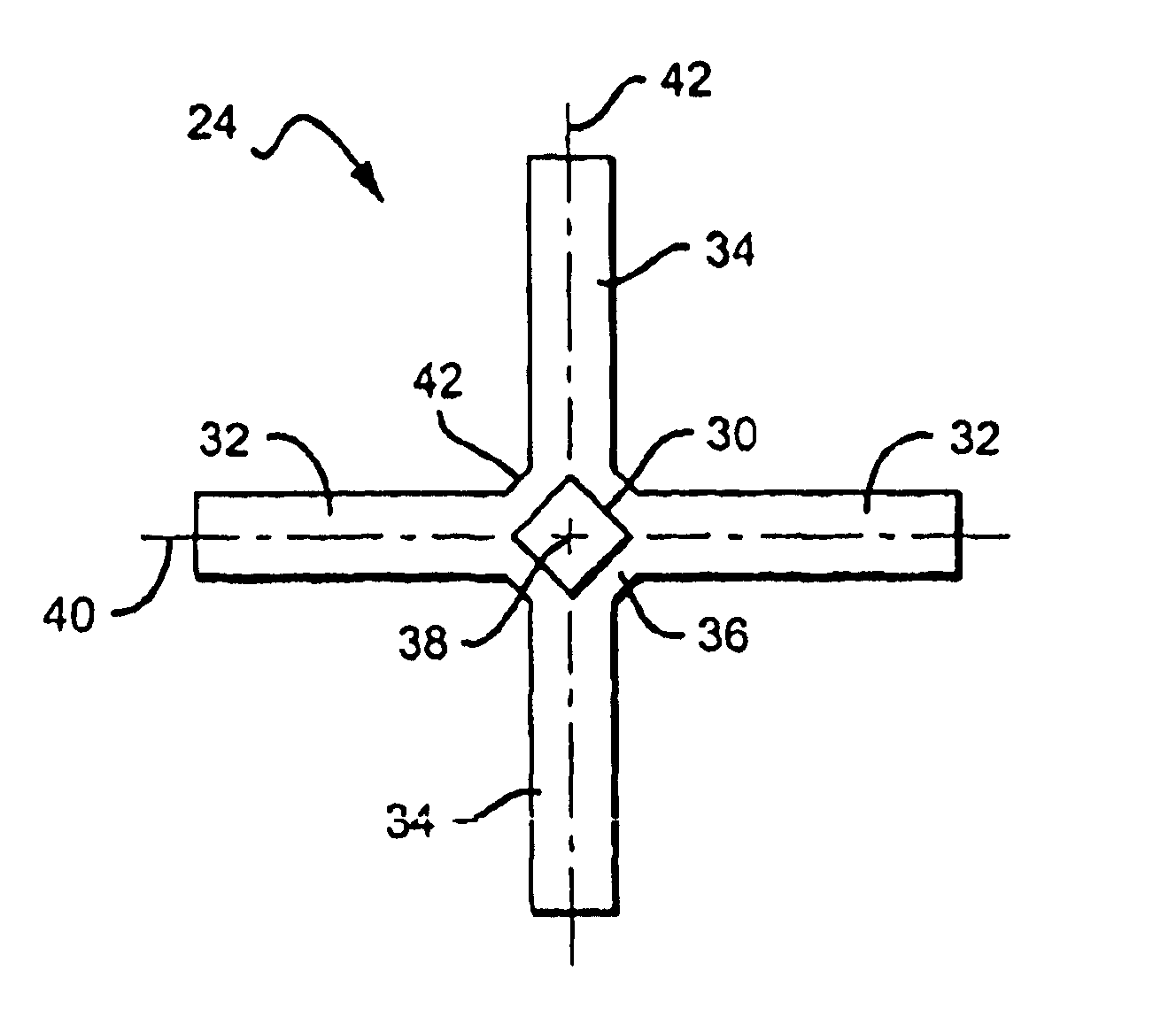
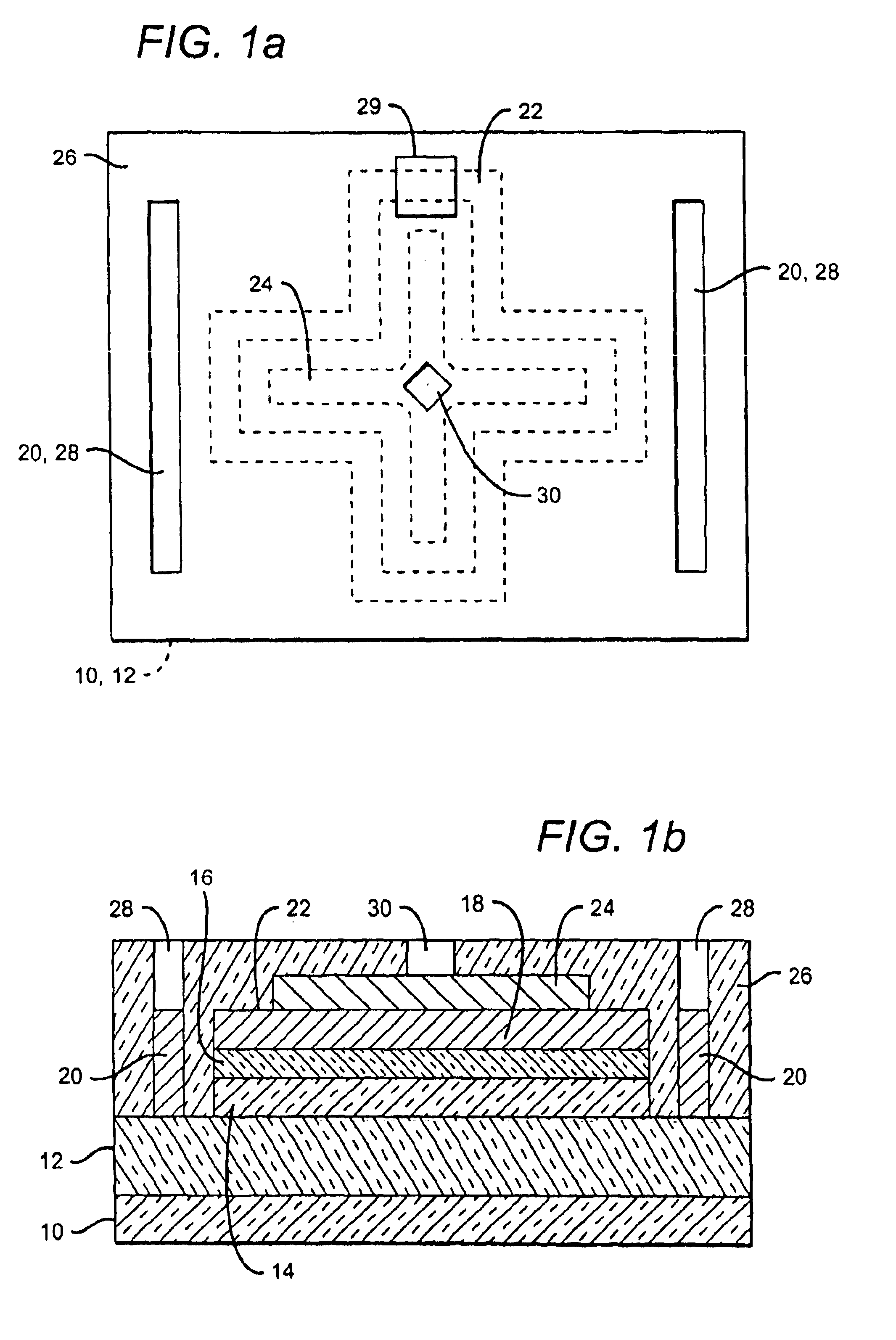
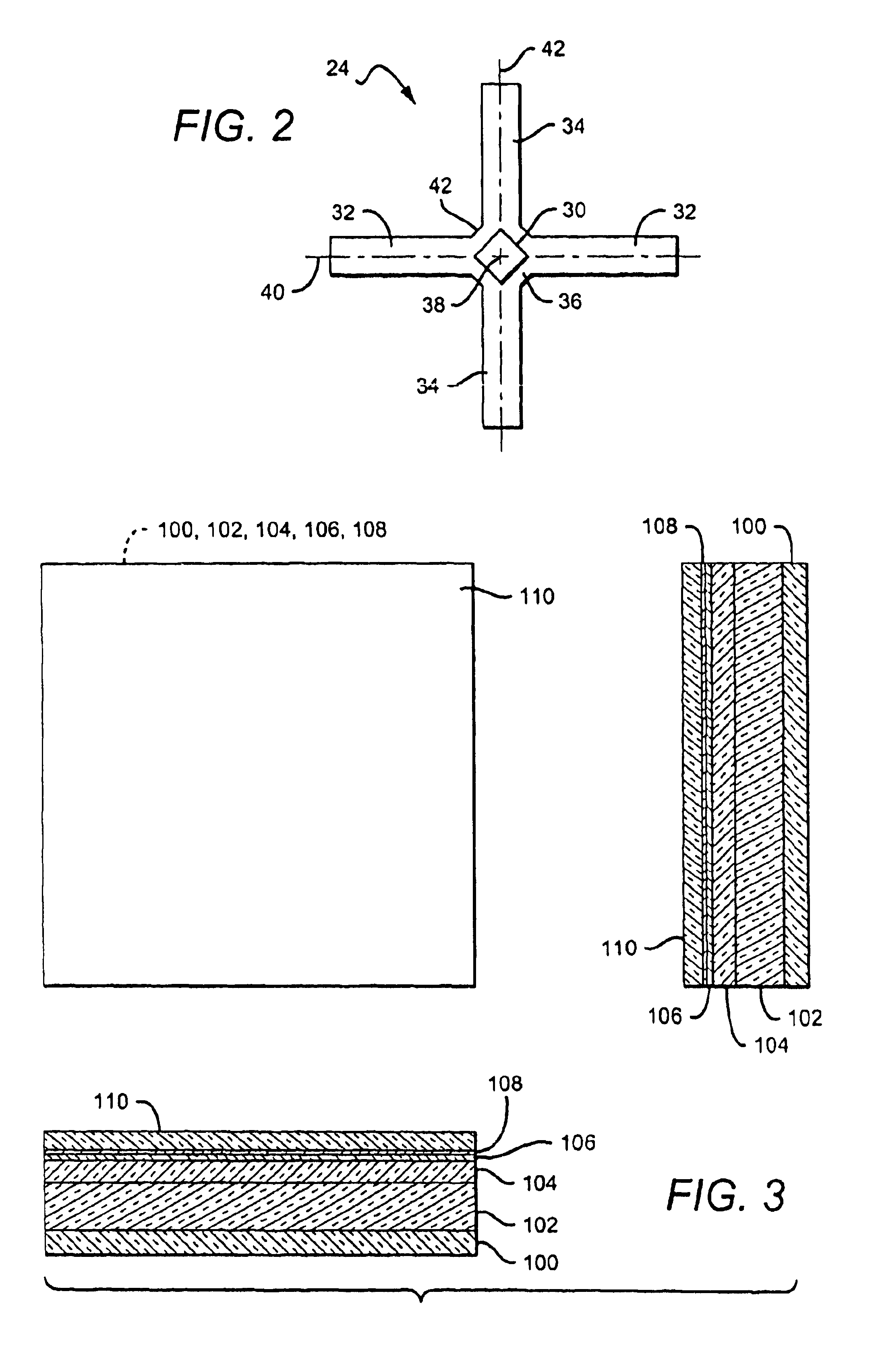
An exemplary embodiment of a BJT device with reduced emitter width is shown in FIGS. 1a (plan view) and 1b (corresponding sectional view). The BJT structure comprises a semi-insulating substrate 10, on top of which is formed a sub-collector 12. A collector 14 is on the sub-collector, a base 16 is atop the collector, and an emitter 18 is formed on the base. Metal contacts 20 are formed on sub-collector 12 to provide a collector terminal for the BJT, and a metal contact 22 on base 16 provides the device's base contact. A cross-shaped metal contact 24 on emitter 18 provides the device's emitter terminal.

An inter-level dielectric layer 26 covers the BJT structure, and vias are formed through layer 26 to access the device contacts: vias 28 provide access to collector contact 20, and a via 29 is formed to provide access to base contact 22. Another via 30 is formed through interlevel dielectric layer 26 to provide access to emitter contact 24. Emitter 18 and emitter contact 24 form an emit...


PUM


Abstract

A BJT device configuration includes an emitter finger and via arrangement which reduces emitter finger width, and is particularly suitable for use with compound semiconductor-based devices. Each emitter finger includes a cross-shaped metal contact which provides an emitter contact; each contact comprises two perpendicular arms which intersect at a central area. A via through an interlevel dielectric layer provides access to the emitter contact; the via is square-shaped, centered over the center point of the central area, and oriented at a 45° angle to the arms. This allows the via size to be equal to or greater than the minimum process dimension, while allowing the width of the emitter finger to be as narrow as possible with the alignment tolerances still being met.

Description

BACKGROUND OF THE INVENTION1. Field of the InventionThis invention relates to the field of bipolar junction transistor (BJT) structures, and particularly to methods of reducing the width of a BJT or HBT device's emitter fingers.2. Description of the Related ArtPower BJTs typically achieve a high current carrying capacity by dividing the device's emitter and emitter contact into a number of separate “fingers”. For best performance, the width of each emitter finger is made as narrow as possible; this enables base resistance (RB) and base-collector capacitance (CBC) to be reduced, which improves the device's RF performance. Heat dissipation is also improved with narrow emitter fingers. Access to each emitter finger is provided with a via formed through an intervening inter-level dielectric layer.The narrowness of an emitter finger is limited by the minimum dimension associated with the fabrication process used to fabricate the device, and by the process's minimum alignment tolerances. ...

Claims


Application Information

Patent Timeline
Patent Type & Authority Patents(United States)
IPC IPC(8): H01L21/331H01L29/417H01L21/02H01L29/66H01L29/08H01L29/423H01L29/02H01L29/40H01L29/737
CPCH01L29/0817H01L29/41708H01L29/7371H01L29/66318H01L29/42304
Inventor LI, JAMES CHINGWEIPIERSON, JR., RICHARD L.BRAR, BERINDER P. S.HIGGINS, JOHN A.
Owner TELEDYNE SCI & IMAGING
Why Eureka
Try Eureka