Polycrystalline silicon and process and apparatus for producing the same

a technology of polycrystalline silicon and process, applied in the field of polycrystalline silicon, can solve the problems of large quantity of flaky and needle-like fine grains, and achieve the effect of achieving efficient results

Inactive Publication Date: 2005-03-01
TOKUYAMA CORP
View PDF21 Cites 27 Cited by
  • Summary
  • Abstract
  • Description
  • Claims
  • Application Information

AI Technical Summary

Benefits of technology

It is a second object of the present invention to provide a method of producing the above polycrystalline silicon with high reproducibility and stability.
The foamed polycrystalline silicon of the present invention can be obtained efficiently by the above apparatus. That is, as hydrogen is existent in the silicon deposition and melting area in the above apparatus, hydrogen can be contacted to a silicon molten liquid formed on the surface of the cylindrical vessel which is a heater and dissolved in the liquid, the resulting product is naturally dropped from the periphery of the opening at the lower end of the cylindrical vessel as droplets, and the droplets are received on a suitable coolant and collected, thereby making it possible to produce the above foamed polycrystalline silicon efficiently.

Problems solved by technology

That is, since polycrystalline silicon cleaves easily, when a nugget obtained by breaking the above silicon rod is further crushed to obtain granular polycrystalline silicon, flaky and needle-like fine grains are easily generated in large quantities.

Method used


Image

  • Polycrystalline silicon and process and apparatus for producing the same
  • Polycrystalline silicon and process and apparatus for producing the same
  • Polycrystalline silicon and process and apparatus for producing the same

Examples


example 1

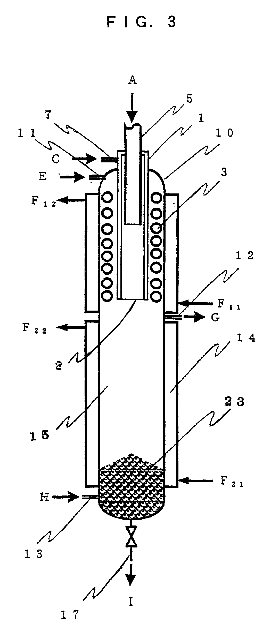
A polycrystalline silicon production apparatus similar to the apparatus shown in FIG. 3 was constructed to continuously produce polycrystalline silicon as follows.

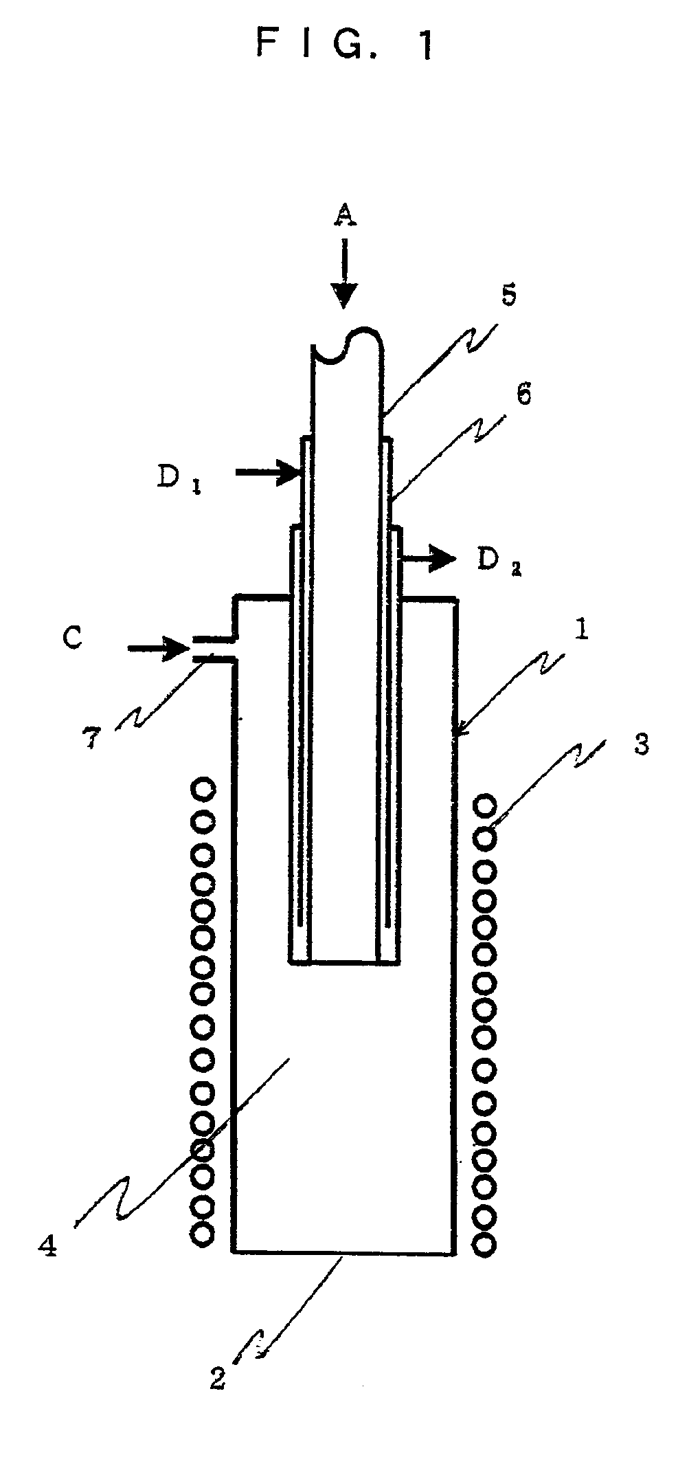
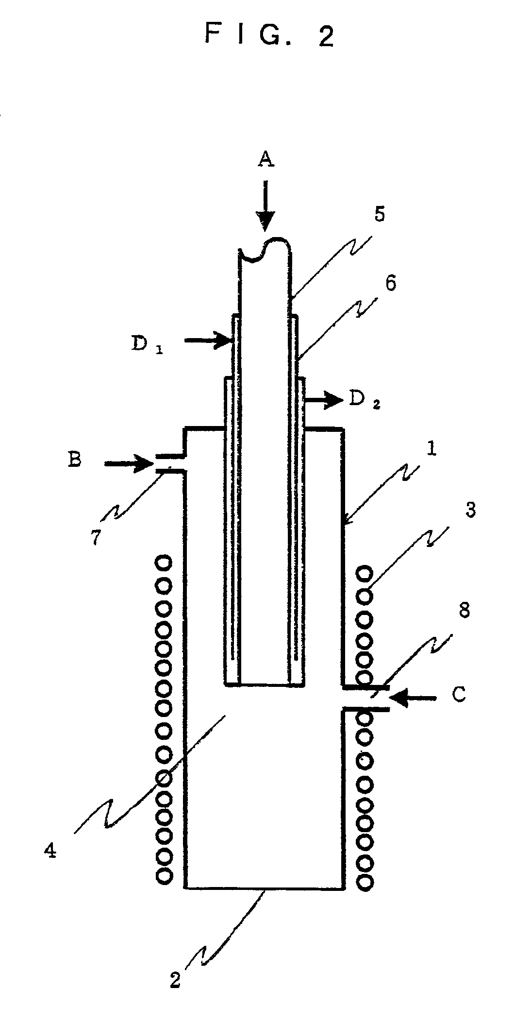
A high-frequency induction heating coil was mounted as the heater 3 around a silicon carbide cylindrical vessel 1 having an opening 2 in a lower portion and an inner diameter of 25 mm and a length of 50 cm from a position 10 cm from the top to the lower end of the cylindrical vessel 1. A stainless steel chlorosilane feed pipe 5 having an inner diameter 10 mm and an outer diameter 17 mm and a jacket structure through which a liquid can be circulated as shown in FIG. 2 was inserted into the cylindrical vessel 1 to a height of 15 cm from the upper end of the cylindrical vessel. The closed vessel 10 had an inner diameter of 500 mm and a length of 3 m and was made from stainless steel.

The periphery of the lower end of the above cylindrical vessel had a shape shown in FIG. 5.

Water was let pass through the cooling jacket of the c...

example 2

Foamed polycrystalline silicon was obtained under the same conditions as in Example 1 except that a silicon molten liquid was formed from silicon tetrachloride as a source material.

When the apparent density of the solidified grain was measured, it was 2.05 g / cm3.

When the grain diameter of the crushed product obtained in the same manner as in Example 1 was measured, the proportion of fine grains passing through a sieve having an opening of 180 μm was 0.2%.

example 3

A silicon molten liquid was formed by filling a graphite cylindrical vessel having a hole in a lower portion with solid silicon and heating at 1,500° C. with high frequency in a hydrogen atmosphere in stead that a silicon molten liquid was formed by reacting trichlorosilane with hydrogen. Further, after it was kept in a molten state for 30 minutes in the presence of hydrogen, it was pressurized with hydrogen from above and dropped from the hole in the lower portion.

The separated and dropped silicon molten liquid droplets were dropped naturally and contacted to a cooling acceptor 9 installed at the lower portion in 0.5 second.

The cooling acceptor 9 was cooled by filling the previously obtained foamed polycrystalline silicon grains therein to maintain its surface temperature at 300° C.

When the apparent density of the solidified grain was measured, it was 2.11 g / cm3.

When the grain diameter of the crushed product obtained in the same manner as in Example 1 was measured by the SK laser, ...


PUM

PropertyMeasurementUnit
apparent densityaaaaaaaaaa
weightaaaaaaaaaa
weightaaaaaaaaaa

Abstract

Foamed polycrystalline silicon having bubbles therein and an apparent density of 2.20 g / cm3 or less. This silicon generates an extremely small amount of fine grains by crushing and can be easily crushed. There is also provided a method of producing foamed polycrystalline silicon. There is further provided a polycrystalline silicon production apparatus in which the deposition and melting of silicon are carried out on the inner surface of a cylindrical vessel, a chlorosilane feed pipe is inserted into the cylindrical vessel to a silicon molten liquid, and seal gas is supplied into a space between the cylindrical vessel and the chlorosilane feed pipe.

Description

FIELD OF THE INVENTIONThe present invention relates to novel polycrystalline silicon, and a process and apparatus for producing the same. More specifically, it relates to foamed polycrystalline silicon which is soft and generates an extremely small amount of fine grains when it is crushed, a method of producing the same stably, and a polycrystalline silicon production apparatus which is suitable for the production of the polycrystalline silicon, capable of producing polycrystalline silicon continuously and stably at a high speed for a long time and extremely useful from an industrial point of view.PRIOR ARTHeretofore, there have been known various methods of producing polycrystalline silicon used as a raw material for a semiconductor or photo voltaic and some of them have already been carried out on an industrial scale.For example, one of the methods is called “Siemens method” that a silicon rod heated at the deposition temperature of silicon by energization is placed in a bell jar ...

Claims


Application Information

Patent Timeline
Patent Type & Authority Patents(United States)
IPC IPC(8): B01J10/00C01B33/03C01B33/00
CPCB01J10/005B01J19/24C01B33/03B01J2219/0009B01J2219/00094Y10T428/2982Y10S117/902Y10T117/1016Y10T117/102B01J2219/00159C30B29/06
Inventor WAKAMATSU, SATORUODA, HIROYUKI
Owner TOKUYAMA CORP
Why Eureka
Try Eureka