Non-linearity correcting method and device for A/D conversion output data

a non-linearity and output data technology, applied in the field of non-linearity correcting methods and devices for a/d conversion output data, can solve the problems of non-linearity error, inability to perform high-precision a/d conversion, and difficulty in using the a/d converting circuit described above in sensing equipment, measuring equipment, etc., and achieve large non-linearity and high precision

Active Publication Date: 2005-03-01
DENSO CORP
View PDF12 Cites 13 Cited by
  • Summary
  • Abstract
  • Description
  • Claims
  • Application Information

AI Technical Summary

Benefits of technology

The present invention has been implemented in view of the foregoing problem, and has an object to provide method and device for linearly correcting non-linearity of A / D conversion output data at low cost without giving consideration to temperature variation.
According to the non-linear correcting device which is constructed to correct the non-linearity of the A / D conversion circuit, non-linearity can be corrected with high precision for an A / D converting circuit having relatively large (remarkable) non-linearity, and the effect Is more remarkable.

Problems solved by technology

The time A / D converting circuit 100 having such non-linearity induces a problem in sensing equipment, etc. to which precise linearity is required, and it is difficult to use the A / D converting circuit described above in sensing equipment, measuring equipment, etc.
However, a non-linearity error caused by the fact that the pulse delay time in the ring gate delay circuit 110 is not proportional to the power supply voltage remains.
Therefore, there is a problem that high-precision A / D conversion cannot be performed.
However, it is required to prepare for a large-capacity ROM and store vast amounts of correction values in the ROM.
However, this method needs to prepare correction values for each of plural temperatures in an estimated temperature range, resulting in increase in scale of ROM and complication of the circuit construction.
Therefore, the cost is increased and thus this method is not practical.
Therefore, even when the method using the correcting ROM as described above is applied as a method of correcting non-linearity of a general A / D converting circuit, the same problem (cost-up due to increase of scale of ROM, etc.) occurs and thus this method is not practical.

Method used


Image

  • Non-linearity correcting method and device for A/D conversion output data
  • Non-linearity correcting method and device for A/D conversion output data
  • Non-linearity correcting method and device for A/D conversion output data

Examples


Embodiment Construction

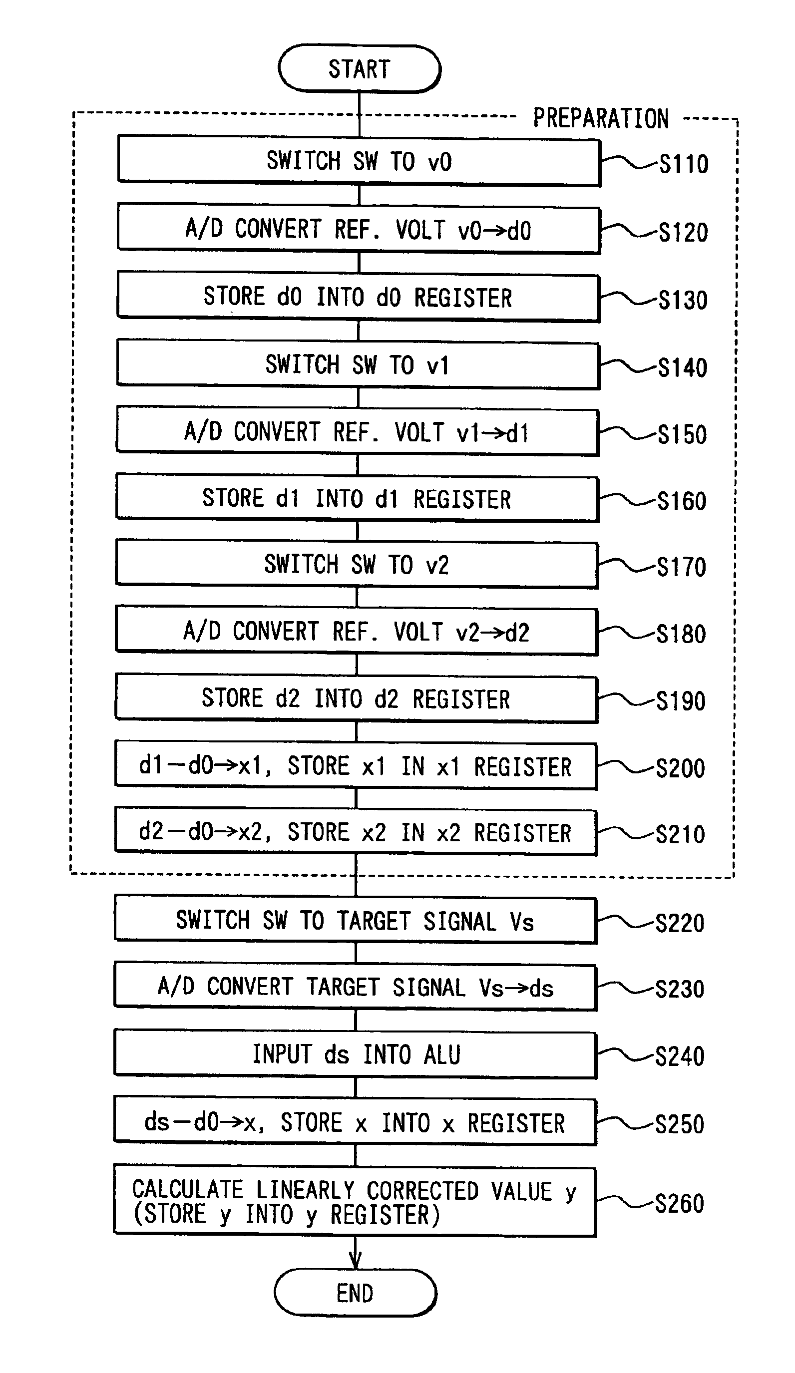
A preferred embodiment according to the present invention will be described hereunder with reference to the accompanying drawings.

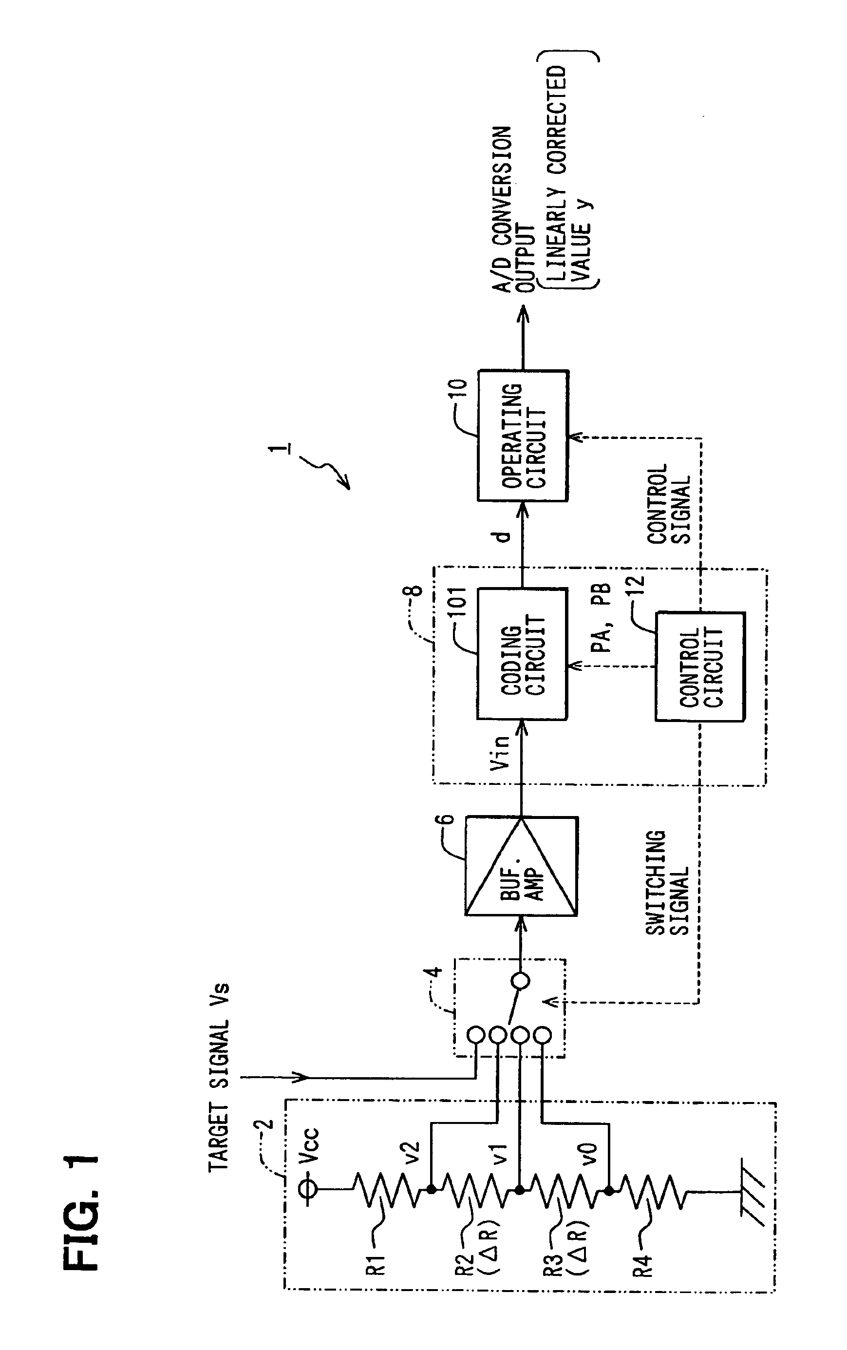
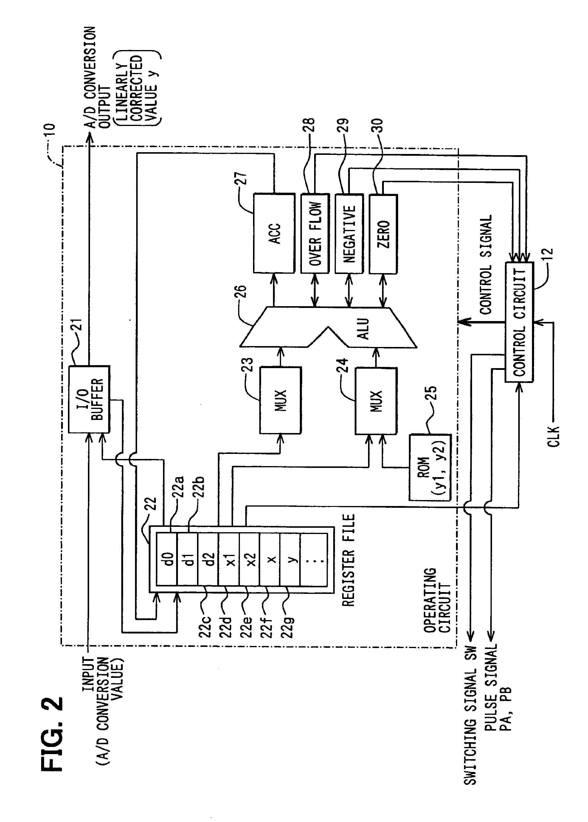
FIG. 1 is a diagram showing the construction of an A / D converting device according to an embodiment of the present invention. The A / D converting device 1 of this embodiment serves to A / D-convert a signal (a signal Vs to be measured; hereinafter referred to as “measurement target signal Vs”) from each semiconductor sensor element (not shown) for detecting a physical quantity, such as a semiconductor type infrared sensor, a semiconductor type pressure sensor or the like, and it is preferably fabricated in one signal processing IC (not shown).

As shown in FIG. 1, it comprises a reference voltage generating circuit 2 for generating three reference voltages v0, v1, v2, an analog multiplexer 4 for selecting and outputting any one of the reference voltages v0, v1, v2 and the measurement target signal Vs from the semiconductor sensor element, a buffer amplifier (a...


PUM


Abstract

Predetermined reference voltages v1, v2 are A / D-converted to achieve corresponding digital data d0, d1, d2. Any reference digital values y1, y2 are set in advance so as to satisfy y1 / y2=(v1−v0) / (v2−v0)=½. Furthermore, calculations of x1=d1−d0 and x2=d2−d0 are carried out to achieve x1, x2. A quadratic curve (quadratic function expression y=f(x)) passing a point D (x1, y1) and a point E (x2, y2) and the origin on the xy coordinate system is set as a linearly correcting expression. A shift value x achieved by subtracting d0 from data ds having non-linearity from the A / D converting circuit is corrected by the linearly correcting expression thus achieved to achieve a linearly corrected value y to ds.

Description

CROSS REFERENCE TO RELATED APPLICATIONThis application is based upon, claims the benefit of priority of, and incorporates by reference the contents of, Japanese Patent Application No. 03-277578 filed on Jul. 22, 2003.FIELD OF THE INVENTIONThe present invention relates to method and device for linearly correcting non-linearity of A / D conversion output data achieved by subjecting an analog signal to A / D conversion in an A / D converting circuit.BACKGROUND OF THE INVENTIONThere has been hitherto known an A / D converter which is equipped with a ring gate delay circuit comprising inverting circuits connected to one another in a ring form as a high-resolution A / D converting circuit having no analog circuit portion, and uses variation of an inverting operation time of each inverting circuit in accordance with a power supply voltage (for example, JP-A-5-259907).An A / D converting circuit disclosed in the above publication (hereinafter referred to as “time A / D converting circuit”) has been propo...

Claims


Application Information

Patent Timeline
Patent Type & Authority Patents(United States)
IPC IPC(8): H03M1/10H03M1/12H03M1/60
CPCH03M1/1042H03M1/12
Inventor TANIZAWA, YUKIHIKO
Owner DENSO CORP
Why Eureka
Try Eureka