Integration method to enhance p+ gate activation

a technology of complementary metaloxide and gate activation, which is applied in the field of semiconductor device fabrication, can solve the problems of device degradation, undesirable degradation of gate oxide integrity, and degrading device properties, and achieves the effect of rapid thermal annealing

Inactive Publication Date: 2005-04-12
TAIWAN SEMICON MFG CO LTD
View PDF10 Cites 7 Cited by
  • Summary
  • Abstract
  • Description
  • Claims
  • Application Information

AI Technical Summary

Benefits of technology

It is yet another object to describe a method to simultaneously activate p+ poly-silicon gate and source / drain regions, while suppressing boron penetration into gate oxide.
In accordance with these objectives, a new process integration method is described to form heavily doped p+ source and drain regions in a CMOS device. After defining the p- and n-well regions on a semiconductor substrate, gate silicon dioxide is deposited and nitrided in a nitrogen-containing atmosphere of gases comprising NH3, NO, and / or NO2. Poly-silicon is then deposited over the nitrided gate dielectric layer and the two NMOS and PMOS gates are formed with anisotropic plasma etching processes. For the p+ doping of the poly-silicon gate and S / D regions around the PMOS gate, B+ ions are then implanted. Cap dielectric layer such as silicon dioxide is then deposited, followed by dopant activation with high temperature rapid thermal annealing. During this anneal step, both poly-silicon gate and source / drain regions are activated. The cap dielectric layer is then used as a resist protective film; it is removed from those areas of the chip that would require formation of electrical contacts. Silicided electrical contacts are then formed in these areas by silicidation processes.

Problems solved by technology

This penetration causes device degradation such as large threshold voltage shifts and saturated current.
Further, undesirable degradation of gate oxide integrity tends to get worse with thinning gate oxide.
However, in the case of PMOS transistor part, pre-doping increases boron ion penetration into the p-channel through the gate oxide thereby degrading the device properties.

Method used


Image

  • Integration method to enhance p+ gate activation
  • Integration method to enhance p+ gate activation
  • Integration method to enhance p+ gate activation

Examples


Embodiment Construction

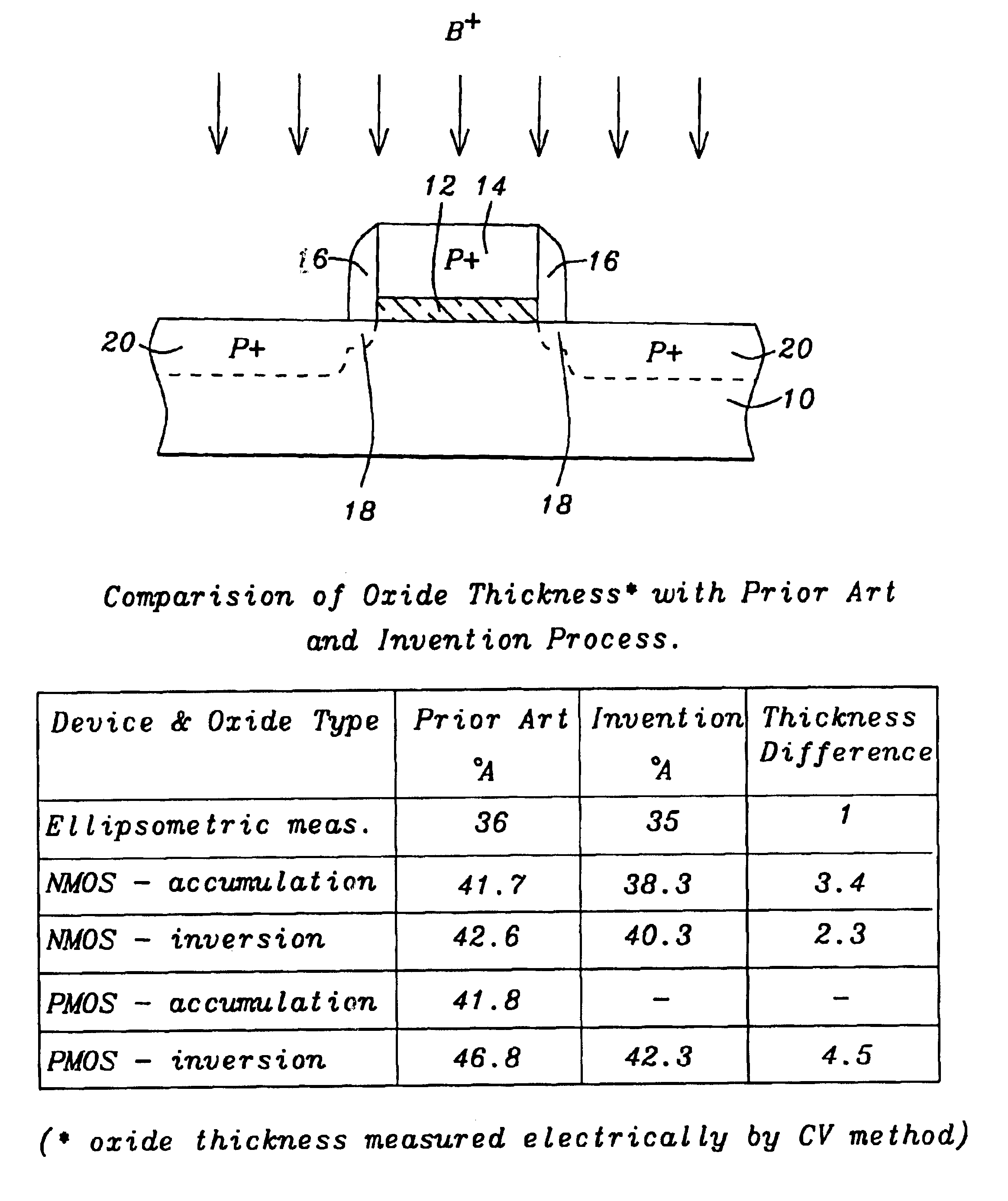
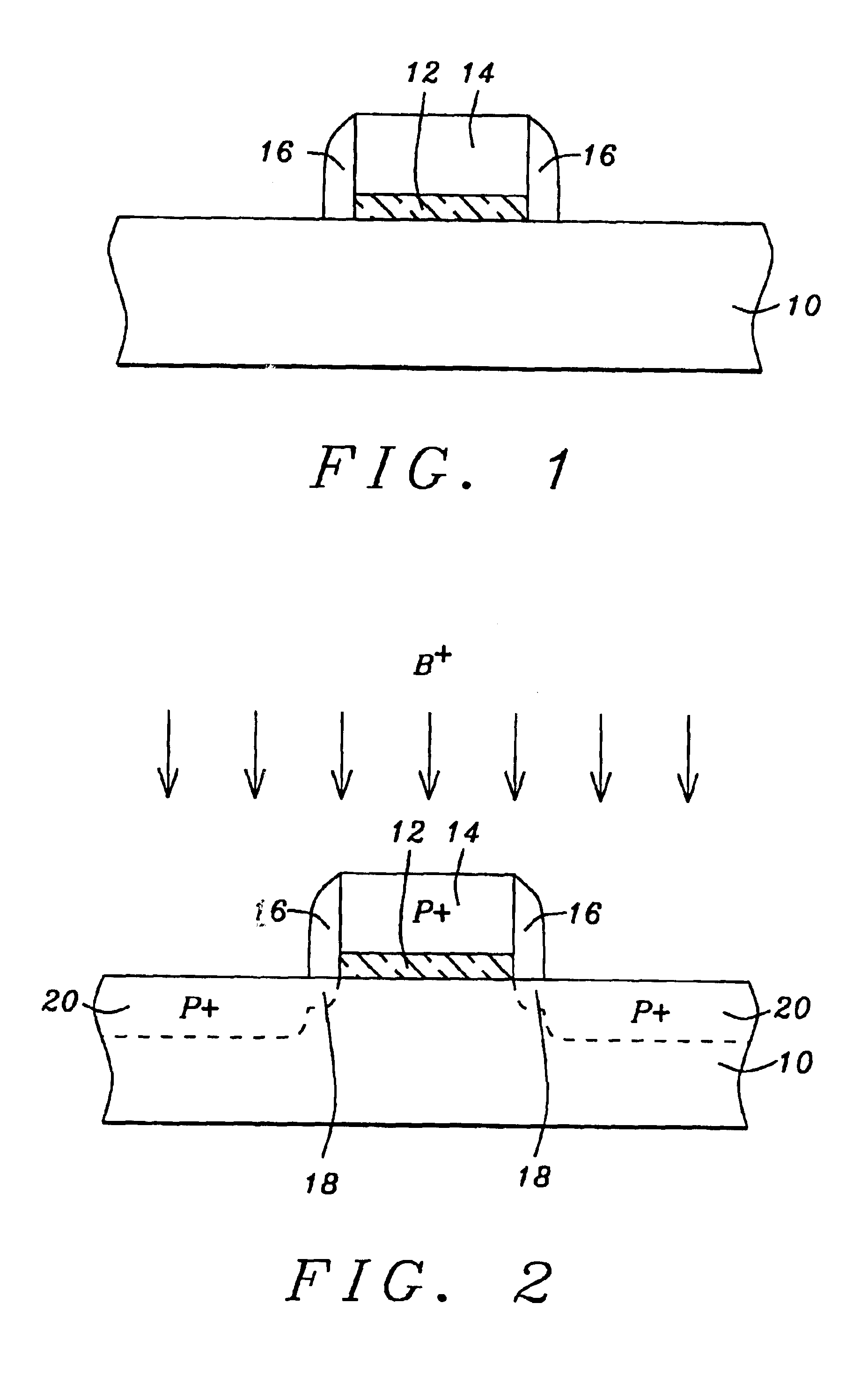
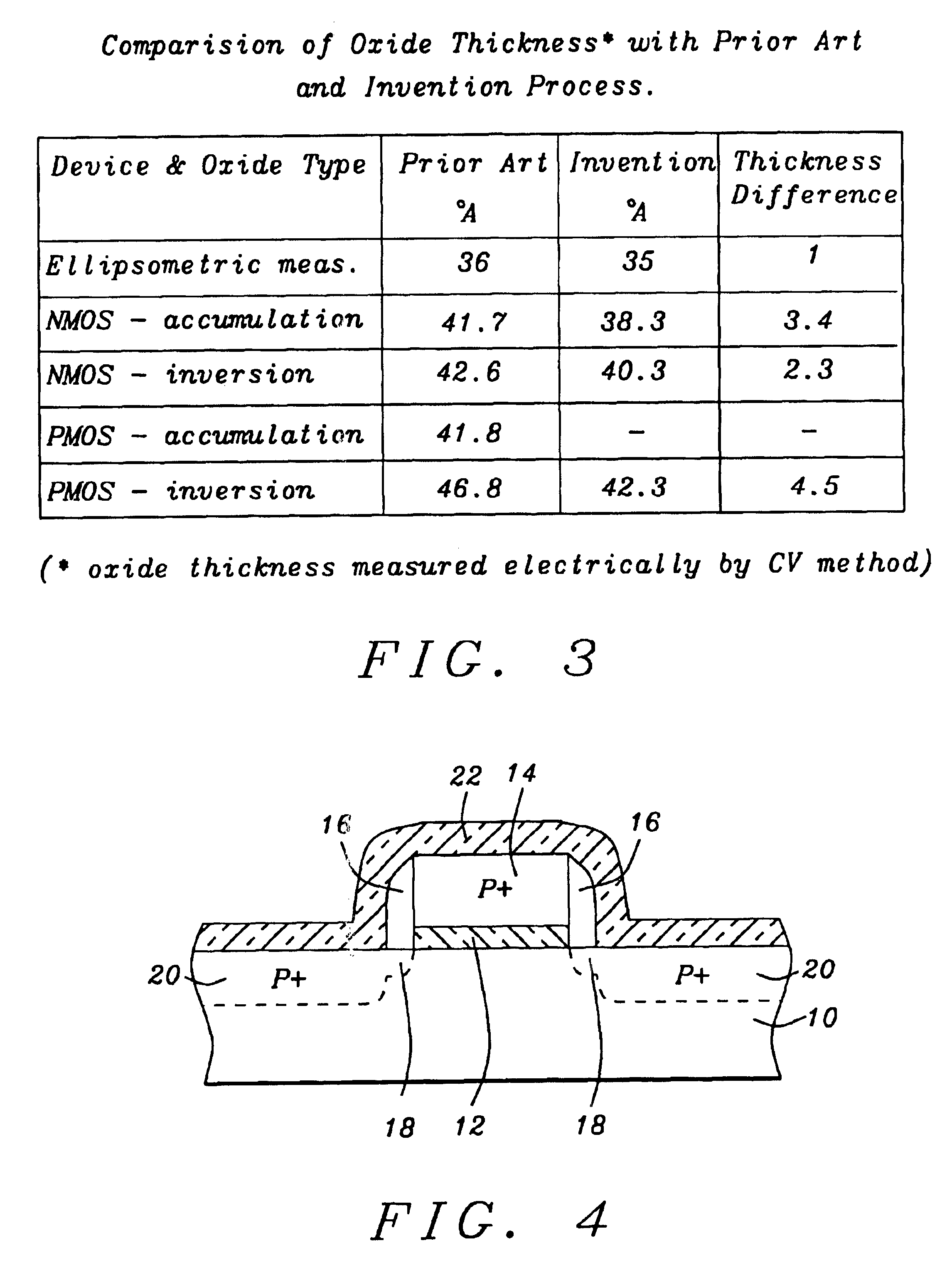
Although the process of this invention can be generally used for activating p+ doped regions in a semiconductor device, the preferred embodiment described herein pertains to the p+ gate activation of a CMOS device. The process steps up to the gate structure formation, being known in the prior art, are not included in this description.

The gate structure, shown in FIG. 1, is formed using the steps of thin film deposition, photolithography, and plasma etching known in the prior art. The gate structure shows semi-conductor substrate, preferably silicon substrate 10; gate dielectric 12, selected from the group of materials comprising silicon dioxide, silicon nitride, nitrided silicon dioxide, oxygen doped silicon nitride, dual gate materials such as silicon dioxide / silicon nitride, and / or high-k gate materials comprising ZrO2, HfO2, and / or other refractory metal oxides; conductor gate 14, selected from the group of materials comprising poly-silicon, doped poly-silicon, dual gates compris...


PUM


Abstract

A new process integration method is described to form heavily doped p+ source and drain regions in a CMOS device. After defining the p- and n-well regions on a semiconductor substrate, gate silicon dioxide is deposited and nitrided in a nitrogen-containing atmosphere. Poly-silicon is then deposited and the two NMOS and PMOS gates are formed. For the p+ doping of the poly-silicon gate and S/D regions around the PMOS gate, B+ ions are then implanted. Cap dielectric layer comprising silicon dioxide is then deposited, followed by dopant activation with high temperature rapid thermal annealing. The cap dielectric layer is then used as resist protective film; it is removed from those areas of the chip that would require formation of electrical contacts. Silicide electrical contacts are then formed in these areas.

Description

BACKGROUND OF THE INVENTION(1) Field of the InventionThis invention relates generally to fabrication of a semiconductor device and more particularly to an integration method to enhance gate activation in a complimentary metal-oxide semiconductor (CMOS) device.(2) Description of the Prior ArtThere is a continuing trend to scale down the dimensions of a semiconductor device for purposes of enhancing device speed, density, and level of integration. In order to increase the speed of a CMOS device for example, channel length or poly-silicon gate width has been decreasing aggressively. Equivalent gate oxide thickness has to correspondingly get thinner to minimize or avoid short channel effects. However, as the gate oxide gets thinner, dopant ions used to increase the conductivity of poly-silicon gate tend to penetrate through the gate and into and through the thin gate oxide layer. This penetration causes device degradation such as large threshold voltage shifts and saturated current. Fur...

Claims


Application Information

Patent Timeline
Patent Type & Authority Patents(United States)
IPC IPC(8): H01L21/265H01L21/70H01L21/28H01L21/02H01L21/8238H01L29/51
CPCH01L21/26513H01L21/28176H01L21/28202H01L21/823842H01L21/823814H01L29/518H01L29/517
Inventor GUO, JYH CHYURN
Owner TAIWAN SEMICON MFG CO LTD
Why Eureka
Try Eureka