Image formation apparatus

a technology of image formation apparatus and spherical tube, which is applied in the direction of television systems, tubes with screens, instruments, etc., to achieve the effect of high display quality configuration

Inactive Publication Date: 2005-04-12
CANON KK
View PDF30 Cites 84 Cited by
  • Summary
  • Abstract
  • Description
  • Claims
  • Application Information

AI Technical Summary

Benefits of technology

It is an object of the present invention to provide an image formation apparatus capable of satisfying large-screen requirements and having a high display-quality configuration.

Problems solved by technology

However, the one using LCD is not of a self light-emitting type and has a problem of requiring a backlight, etc., and therefore a display apparatus of a self light-emitting type is needed.

Method used


Image

  • Image formation apparatus
  • Image formation apparatus
  • Image formation apparatus

Examples


examples 2 and 3

As Examples 2 and 3, an electron source with many plane type surface-conduction emission devices arranged in a simple matrix as shown in FIG. 18 was formed using printed wiring and combined with an image forming member to make up an image forming apparatus.

Referring to FIG. 89, the configuration and the production procedure of this example will be described below.

examples 1 and 2

will be described.

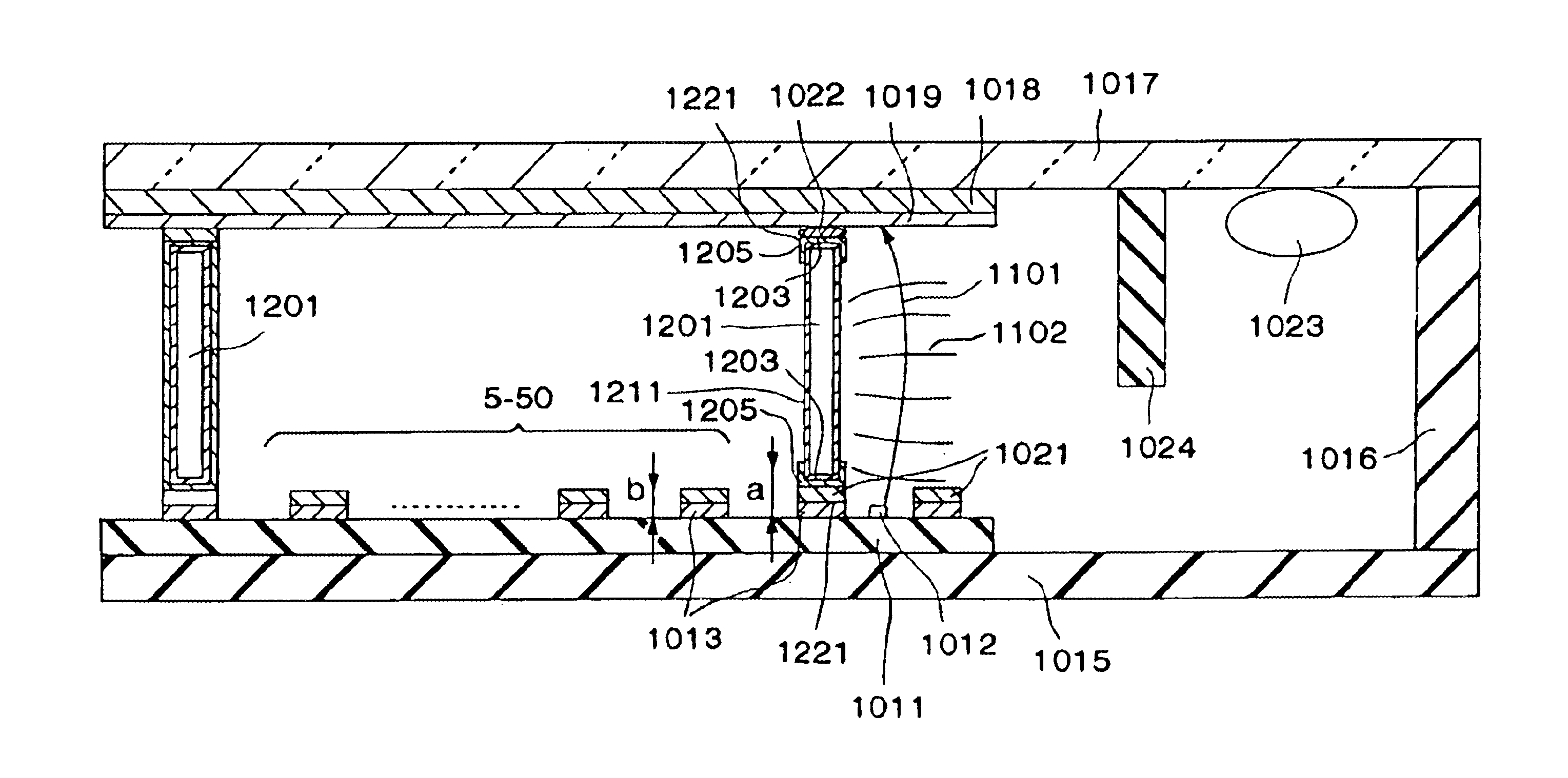
FIGS. 89a to 89f are process drawings showing the production procedure of this example (here, a portion wired in matrix of 3×3, total 9, of devices situated at a corner of the image formation area as part of electron source on unillustrated substrate is shown). In FIGS. 89a to 89f, Numerals 212 and 213, denote a pair of device electrodes, 214 a conductive film for the formation of an electron emission part, 216 a first wiring layer, 217 a second layer and 218 an interlayer insulating film provided between the first wiring layer 216 and the second wiring layer 217. All the total devices are set in a configuration of 720 devices arranged in row and 240 devices arranged in column.

First, on a previously washed substrate (here, a soda lime glass substrate is used), printing and baking of device electrodes is performed to form a pair of electrodes 212 and 213 (FIG. 89a). In this example, a thick-film print method was used as a method for forming a film. The thick-film pa...

example 5

An image forming apparatus according to this example is fundamentally characterized in that the wiring is constructed by the screen print like FIGS. 97 and 101. One procedure of a method for manufacturing an image forming apparatus according to this example is shown in FIGS. 102a to 102d. Referring to FIG. 97, FIG. 100 and FIGS. 102a to 102d, a fundamental construction method and a manufacturing method of an image forming apparatus according to this example will be described below.

Step-a:

As with Example 1 of 17th Configuration, device electrodes 3202 and 3203 are formed on a cleaned glass substrate (FIG. 102a).

Step-b:

As with Example 1 of 17th Configuration, the wiring 3206 is formed. Here, a conductive member 3209 is simultaneously formed at a given position, i.e. at outer four corners of the image forming area (FIG. 102b). Incidentally, the distance between the conductive member 3209 and wires 3206 was set to approx. 200 μm or less.

Step-c:

Next, as with Example 1 of 17th Configurati...


PUM


Abstract

An image formation apparatus is disclosed which includes, within an enclosure configured by a pair of substrates placed face to face and an external frame placed between the substrates, an electron source placed on one of the pair of substrates, an image formation material placed on the other substrate, and spacers placed between the substrates, characterized in that the spacers and the external frame is conductive and device is provided for electrically connecting the spacers and the external frame so that the equipotential surfaces between the spacers and the external frame are quasi-parallel when driven.

Description

TECHNICAL FIELDThe present invention relates to an image formation apparatus provided with an electron beam source substrate and a light-emitting display plate placed face to face that forms an image by supplying electrons emitted from the electron beam source substrate according to image information to the light-emitting display plate.BACKGROUND ARTImage display apparatuses equipped with an electron emission cathode of various configurations are conventionally proposed. As an example, the one having a structure whose cross-sectional view is shown in FIG. 1 is known. The display apparatus shown in FIG. 1 is a full-color display apparatus and has multiple stripe-shaped anode electrodes 11106 provided on the inner surface of an anode substrate 11101 and on the anode electrodes 11106 are formed surfaces on which fluorescent materials that emit R, G and B lights are sequentially deposited. On the other hand, on a cathode substrate 11102 facing the anode substrate 11101 are provided FEC ...

Claims


Application Information

Patent Timeline
Patent Type & Authority Patents(United States)
IPC IPC(8): G09G3/22H01J29/00H01J31/12H01J29/86H01J29/92H01J29/02H04N9/30H04N9/12H04N5/70G09G5/02H04N5/44G09G3/20
CPCG09G3/2011H04N9/30G09G3/22H01J1/316H01J29/02H01J29/028H01J29/04H01J29/085H01J29/86H01J29/864H01J29/90H01J29/92H01J29/94H01J31/127H04N5/70G09G5/02G09G2310/0229G09G2310/0267G09G2310/027G09G2320/0276G09G2320/0626G09G2330/02G09G2330/027G09G2330/04G09G2340/125H01J2201/3165H01J2201/319H01J2329/02H01J2329/0489H01J2329/323H01J2329/8625H01J2329/863H01J2329/864H01J2329/8645H01J2329/8655H01J2329/866H01J2329/90H01J2329/92H04N7/012H04N9/12G09G3/2014
Inventor MIYAZAKI, TOSHIHIKOONO, TAKEOMITSUTAKE, HIDEAKIHASEGAWA, MITSUTOSHIYAMAGUCHI, EIJIYAMADA, SHUJITODOKORO, YASUYUKI
Owner CANON KK
Why Eureka
Try Eureka