Method for circuit protection during radiation sterilization

a radiation sterilization and circuit protection technology, applied in the field of circuit protection devices and methods, can solve the problems of chemical sterilization, autoclaving, chemical sterilization, etc., and achieve the effect of reducing the number of radiation sterilization units, increasing the importance and difficulty of sterilization of medical devices, and increasing the complexity of devices

Inactive Publication Date: 2005-04-19
MINIMED
View PDF31 Cites 10 Cited by
  • Summary
  • Abstract
  • Description
  • Claims
  • Application Information

AI Technical Summary

Problems solved by technology

Over the years, sterilization of medical devices has become more important and difficult.
For instance, the devices are becoming more complicated and use many different materials, such that autoclaving, chemical sterilization, or the like, is no longer possible, since the processes would likely destroy the materials of the medical device or fail to reach areas not readily accessible after construction of the medical device.
In addition, many medical devices are now being used in the home by patients, and these patients generally do not have the equipment necessary to perform the required sterilization.
Thus, on-site sterilization has become difficult or impossible to perform at the site of use.
However, additional sterilization is often required.
Heat and chemical sterilization cannot always be used due to possible destruction of the various materials.
Although radiation sterilization has solved many sterilization issues, it is difficult to sterilize complicated devices containing electronic circuits, since the radiation has the capability to damage or destroy semiconductor circuit elements.
One approach is to remove the circuits prior to sterilization, but this still raises issues of sterilization when the device is reassembled.

Method used


Image

  • Method for circuit protection during radiation sterilization
  • Method for circuit protection during radiation sterilization
  • Method for circuit protection during radiation sterilization

Examples


Embodiment Construction

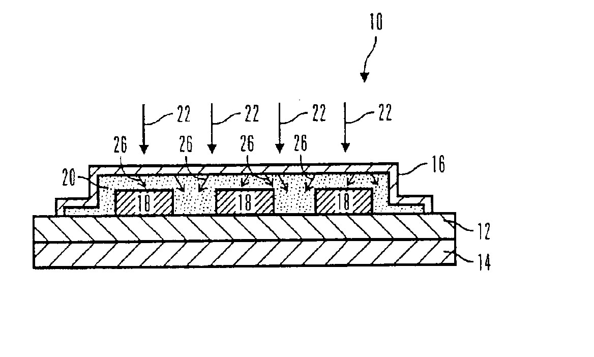
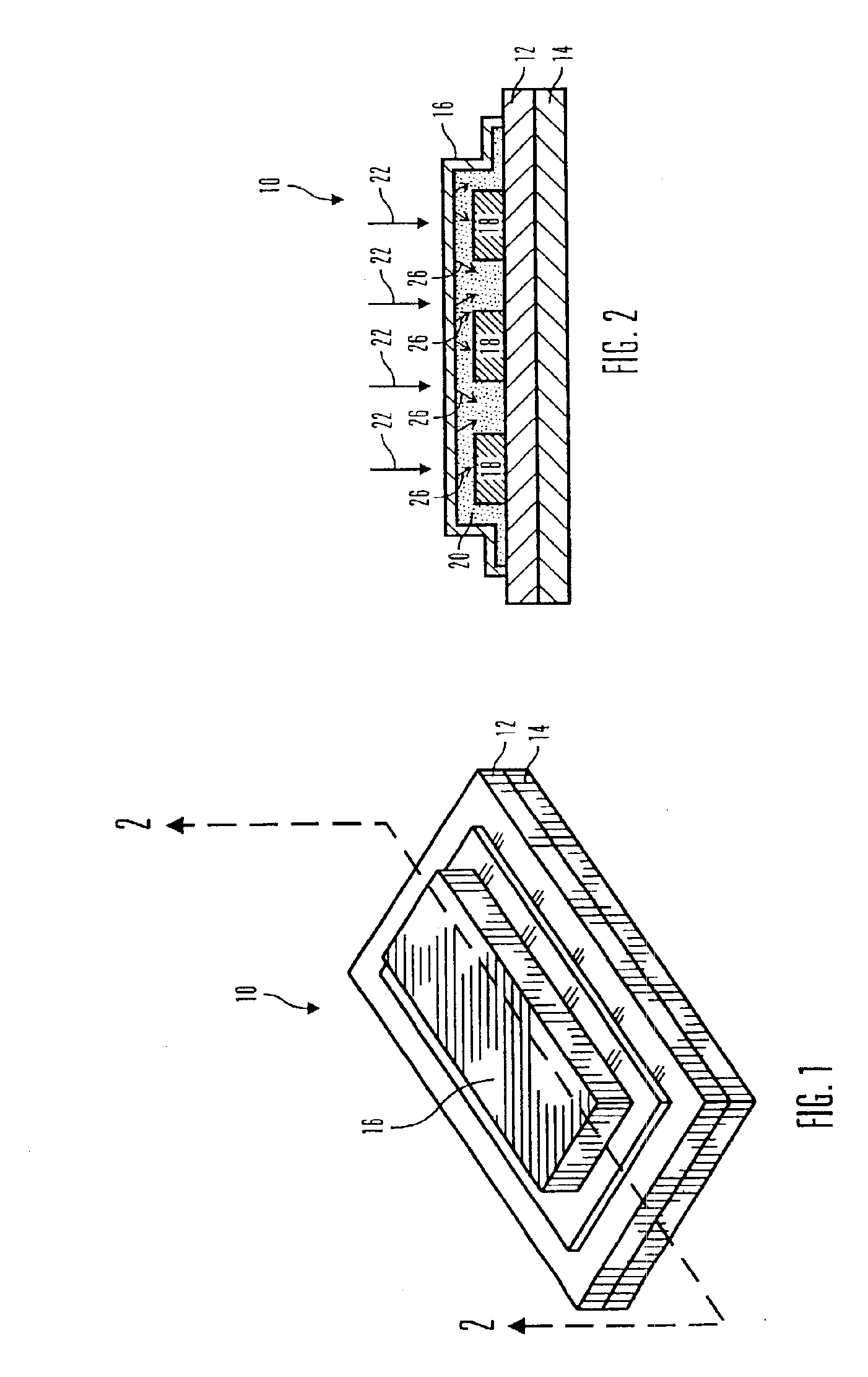
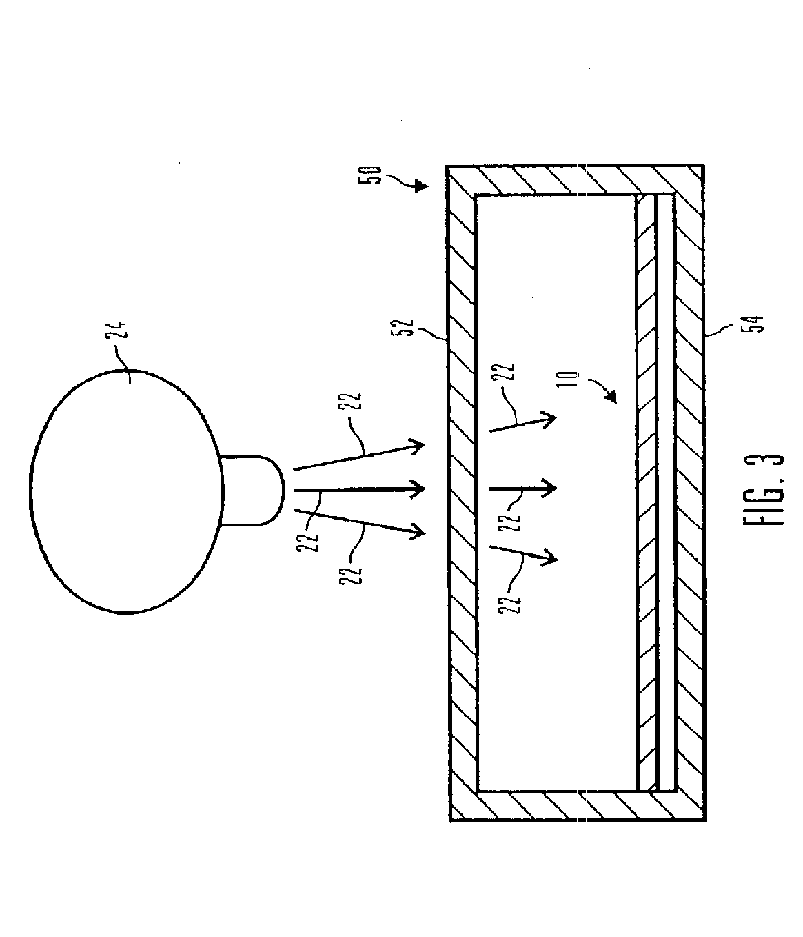
[0026]As shown in the drawings for purposes of illustration, the invention is embodied in a circuit protection device and method for use during E-beam sterilization to permit sterilization of a medical device containing semiconductor circuit elements. In preferred embodiments of the present invention, the circuit protection device forms a permanent part of a circuit board, which permits sterilization of the medical device and circuit board after final assembly. However, it will be recognized that further embodiments of the invention may be used to protect circuit elements that are sterilized prior to final assembly in a medical device. The circuit protection device is primarily adapted for use in medical device for external use. However, alternative embodiments may be used in medical devices to be placed internally within the patient or for both internal and external use. Preferred embodiments are for use with medication infusion devices. However, alternative embodiments may be used...


PUM

PropertyMeasurementUnit
energyaaaaaaaaaa
energy absorbingaaaaaaaaaa
electricalaaaaaaaaaa

Abstract

A circuit protection device for protection of sensitive components during high energy radiation sterilization that includes a support substrate and a protective housing. The substrate supports the sensitive components. The protective housing is hermetically coupled to the support substrate to seal the sensitive components within the protective housing. Preferably, the protective housing stops high energy used in the high energy sterilization from damaging the sensitive components from a predetermined exposure level of high energy sterilization. The circuit protection device may further include a protective conductor that is coupled to the support substrate on a side which is opposite the protective housing to prevent high energy from entering the opposite side of the support substrate. The circuit protection device can also include an energy absorbing material contained within an area sealed by the protective housing to absorb high energy byproducts produced by the protective housing stopping the high energy used in the high energy sterilization. Preferably, the support substrate is a circuit board, and the sensitive elements are semiconductors. Also, the high energy sterilization is E-beam sterilization and the high energy are electrons, and the high energy byproducts are x-rays.

Description

CROSS-REFERENCE TO RELATED APPLICATIONS[0001]This application is a continuation application of U.S. patent application Ser. No. 09 / 556,227, filed Apr. 24, 2000, now U.S. Pat. No. 6,594,156, and entitled “DEVICE AND METHOD FOR CIRCUIT PROTECTION DURING RADIATION STERILIZATION” which is incorporated herein by reference.FIELD OF THE INVENTION[0002]This invention relates to circuit protection devices and methods, and in particular embodiments, to circuit protection devices and methods for use during radiation sterilization of devices containing electronic circuits.BACKGROUND OF THE INVENTION[0003]Over the years, sterilization of medical devices has become more important and difficult. At one time it was possible to sterilize most medical devices at the site of use, since the devices were relatively simple, such as reusable syringes, scalpels, scissors or the like. In addition, the medical devices were often used in a doctor's office, hospital, or the like, that included sophisticated st...

Claims


Application Information

Patent Timeline
Patent Type & Authority Patents(United States)
IPC IPC(8): A61L2/08A61L2/26
CPCA61L2/081A61L2/087A61L2/26H01L23/556A61L2/082Y10T29/49117A61L2202/24H01L2924/145H01L25/0655H01L2924/1435H01L2924/1438H01L2924/0002Y10T29/4913Y10T29/49137Y10T29/49144H01L2924/00
Inventor VAN ANTWERP, WILLIAM P.KARRE, SHEANAPROKOP, ADRIANSTINSON, SARA AKIKOFONG, JASONROSENBERG, JAMES J.
Owner MINIMED
Why Eureka
Try Eureka