Voltage island chip implementation

Inactive Publication Date: 2005-04-19
GLOBALFOUNDRIES INC
View PDF6 Cites 95 Cited by
  • Summary
  • Abstract
  • Description
  • Claims
  • Application Information

AI Technical Summary

Benefits of technology

[0006]It is therefore an object of the present invention to provide a method of designing an integrated circuit chip that supplies a chip design and partitions elements of the chip design according to similarities in voltage requirements and timing of power states of the elements to create voltage islands. The invention outputs a voltage i

Problems solved by technology

This increasing power density in turn drives the need for more expensive packaging, complex cooling solutions and decreased reliability due to increased temperatures.
This decrease in Vt and Tox then drives si

Method used


Image

  • Voltage island chip implementation
  • Voltage island chip implementation
  • Voltage island chip implementation

Examples


Embodiment Construction

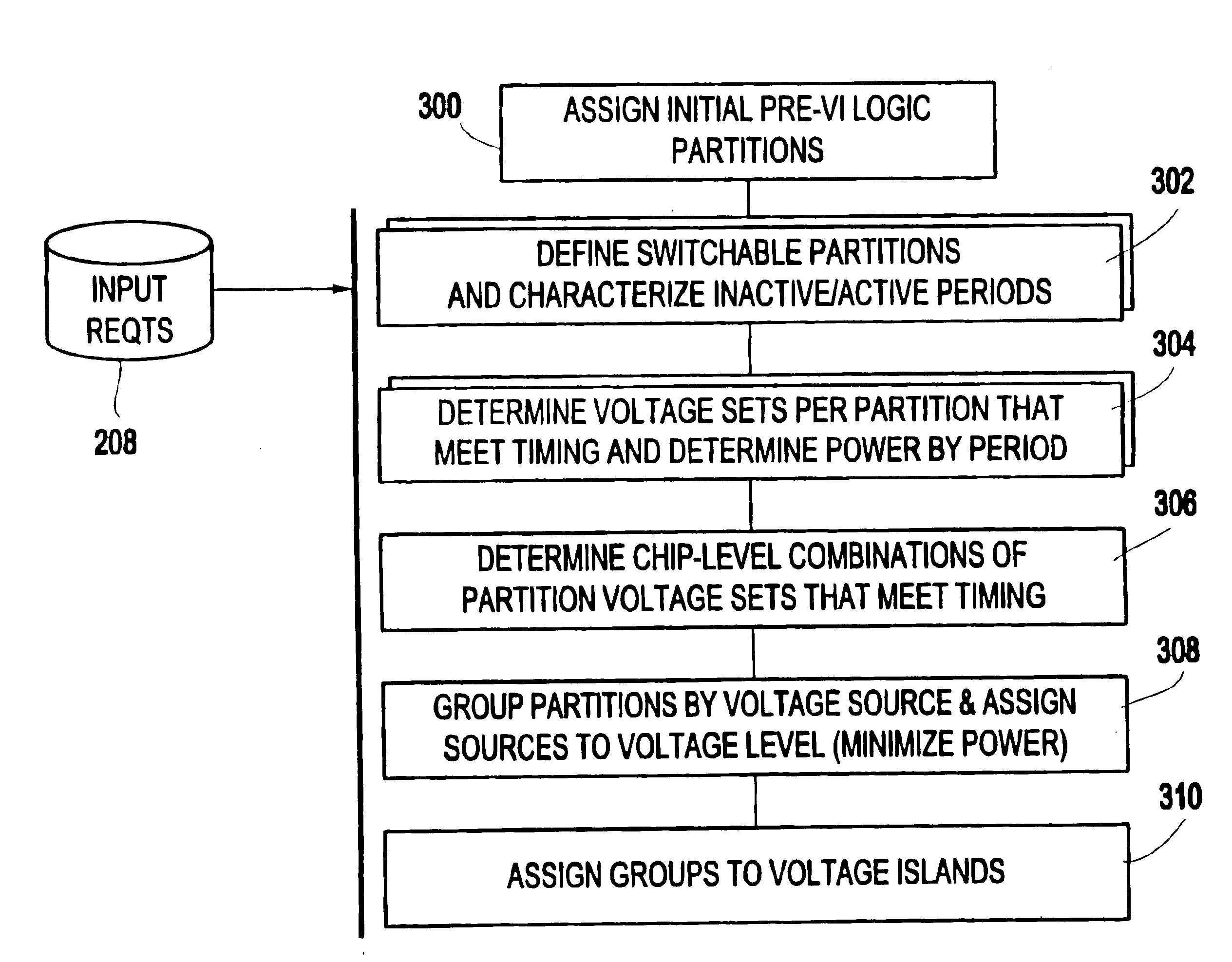
[0026]The power challenges posed by advanced technologies force system designers to make choices concerning device structures and voltage levels for the functions they are designing. In previous generations, large functional blocks were not integrated on the same chip, so these choices could be made independently for each block. High levels of integration supported by system-on-a-chip (SoC) enabling technology drive single chip implementations, where traditional approaches to power distribution and performance optimization fail to provide the flexibility of voltage and technology optimization of the previously disintegrated solution.

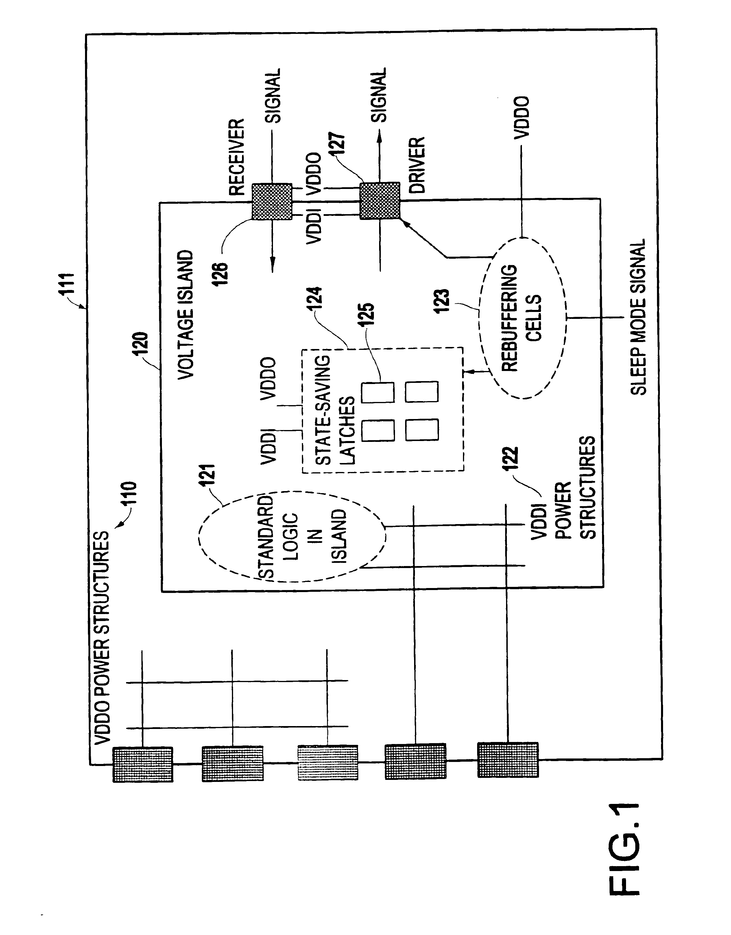
[0027]The invention divides each semiconductor chip into individual functional blocks (voltage islands). These voltage islands of the SoC design can have power characteristics unique from the rest of the design and, with the invention, can be optimized accordingly.

[0028]An SoC architecture based on Voltage Islands uses additional design components to ens...


PUM


Abstract

A method and structure for designing an integrated circuit chip supplies a chip design and partitions elements of the chip design according to similarities in voltage requirements and timing of power states of the elements to create voltage islands. The invention outputs a voltage island specification list comprising power and timing information of each voltage island; and automatically, and without user intervention, synthesizes power supply networks for the voltage islands.

Description

CROSS-REFERENCE TO RELATED APPLICATIONS[0001]This application is a division of U.S. application Ser. No. 10 / 065,201 filed Sep. 25, 2002 now U.S. Pat. No. 6,820,240.BACKGROUND OF THE INVENTION[0002]The present invention generally relates to integrated circuits and more particularly to an improved integrated circuit design and method which utilizes voltage islands that operate at independent voltages and can be selectively gated to reduce power consumption.DESCRIPTION OF THE RELATED ART[0003]As technology scales for increased circuit density and performance, the need to reduce power consumption increases in significance as designers strive to utilize the advancing silicon capabilities. The consumer product market further drives the need to minimize chip power consumption.[0004]The total power consumed by conventional CMOS circuitry is composed of two primary sources. The first is active power consumed by circuits as they switch states and either charge or discharge the capacitance ass...

Claims


Application Information

Patent Timeline
IPC IPC(8): G06F17/50
CPCG06F17/5045G06F30/30
Inventor BEDNAR, THOMAS R.GOULD, SCOTT W.LACKEY, DAVID E.STOUT, DOUGLAS W.ZUCHOWSKI, PAUL S.
Owner GLOBALFOUNDRIES INC
Why Eureka
Try Eureka