Specimen sensing and edge gripping end effector

a technology of edge gripping end and specimen, which is applied in the field of specimen handling apparatus and method, can solve the problems of backside damage to the wafer, contamination of the other wafers, scratches on the backside of the wafer, etc., and achieve the effect of reducing specimen damage and producing contaminan

Inactive Publication Date: 2005-05-24
BOOKS AUTOMATION US LLC
View PDF57 Cites 26 Cited by
  • Summary
  • Abstract
  • Description
  • Claims
  • Application Information

AI Technical Summary

Benefits of technology

[0007]An object of this invention is, therefore, to provide a specimen handling device that minimizes specimen damage and the production of contaminant particles.
[0008]Another object of this invention is to provide a semiconductor wafer handling device that can quickly and accurately transfer semiconductor wafers between a wafer cassette and a wafer processing station.
[0011]The end effectors are generally spatula-shaped and have a proximal end that is operably connected to a robot arm. The active contact point is located at the proximal end, which allows the end effector to be lighter, stronger, and more slender than end effectors having moving mechanisms that may not fit between adjacent wafers in a cassette. The lack of moving mechanisms that could be located over a wafer further causes the end effector to produce less contamination within the cassette. Additionally, locating the active contact point at the proximal end of the end effector ensures that it is remote from harsh conditions such as heated environments and liquids.
[0013]Alternative embodiments of the end effector include flat or inclined, narrow or arcuate rest pads onto which the wafer is initially loaded. The narrow and arcuate inclined rest pad embodiments assist in centering and gripping the wafer between the active contact point and the distal rest pads. The arcuate rest pads more readily accommodate gripping and handling flatted wafers.
[0014]Embodiments of the end effectors further include fiber optic light transmission sensors for accurately locating the wafer edge and bottom surface. Three alternative embodiments include placing the wafer edge and bottom sensors at the proximal end of the end effector; placing the edge sensors at the proximal end and the bottom sensors at the distal end of the end effector; and placing a combined edge and bottom sensor at the distal end of the end effector. In all three embodiments, the sensors provide robot arm extension, elevation, and positioning data that support methods of rapidly and accurately placing a wafer on and retrieving a wafer from a wafer transport stage or a process chamber, and placing a wafer in and retrieving a wafer from among a stack of closely spaced waters stored in a wafer cassette. The methods effectively prevent accidental contact between the end effector and adjacent wafers stacked in a cassette or a wafer resting on a processing device while effecting clean, secure gripping of the wafer.

Problems solved by technology

Unfortunately, transferring the wafer among the cassette, robot arm, and processing stations, such as a prealigner, may cause backside damage to the wafer and contamination of the other wafers in the cassette because intentional engagement as well as inadvertent touching of the wafer may dislodge particles that can fall and settle onto the other wafers.
Wafer backside damage can include scratches as well as metallic and organic contamination of the wafer material.
Moreover, the wafer being transferred may be scratched or abraded on its backside, resulting in wafer processing damage.

Method used


Image

  • Specimen sensing and edge gripping end effector
  • Specimen sensing and edge gripping end effector
  • Specimen sensing and edge gripping end effector

Examples


first embodiment

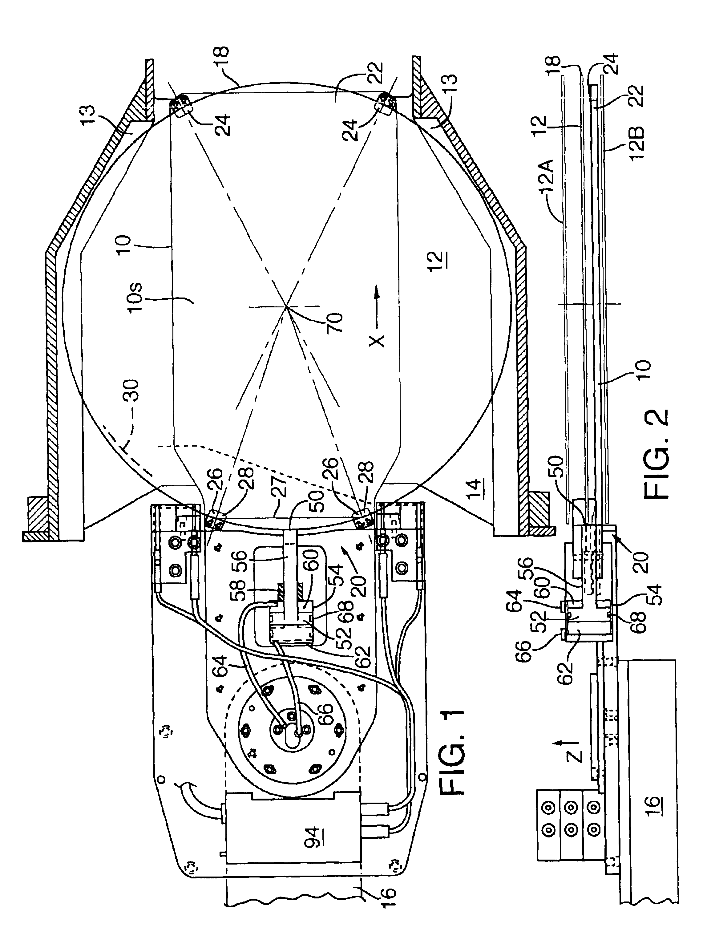
[0034]FIGS. 1 and 2 show a spatula-shaped end effector 10 of this invention for transferring semiconductor wafers, such as a wafer 12 (shown transparent to reveal underlying structures), to and from a wafer cassette 14. End effector 10 is adapted to receive and securely hold wafer 12 and transfer it to and from cassette 14 for processing. FIG. 2 shows that end effector 10 is particularly adapted for retrieving and replacing wafer 12 from among closely spaced wafers, such as wafers 12, 12A, and 12B, which are shown as they might be stacked in slots 13 of wafer cassette 14, or from a lowermost slot 13 of wafer cassette 14. Wafers having diameters of less than 150 mm are typically spaced apart at a 4.76 mm ({fraction (3 / 16)} inch) pitch distance; 200 mm diameter wafers are typically spaced apart at a 6.35 mm (¼ inch) pitch distance; and 300 mm wafers are typically spaced apart at a 10 mm (0.394 inch) pitch distance.

[0035]End effector 10 is operably attached to a robot arm 16 (a portion...

second embodiment

[0068]FIGS. 7 and 8 show a spatula-shaped end effector 110 of this invention for transferring semiconductor wafers, such as wafer 12 (shown transparent to reveal underlying structures), to and from wafer cassette 14 (not shown in this view). End effector 110 is similar to end effector 10 but is further adapted to sense the bottom surface of a wafer stored in wafer cassette 14 without protruding into the cassette. FIG. 8 shows that end effector 110 is particularly adapted for retrieving and replacing wafer 12 from among closely spaced apart wafers, such as wafers 12, 12A, and 12B, which are shown as they might be stacked in wafer cassette 14.

[0069]End effector 110 is operably attached to robot arm 16. In general, end effector 110 senses the bottom surface of wafer 12 before entering wafer cassette 14 to retrieve wafer 12 from between wafers 12A and 12B. End effector 110 is then finely positioned by robot arm 16 and actuated to grip periphery 18 of wafer 12, remove wafer 12 from casse...

third embodiment

[0103]FIGS. 12, 13, and 14 show a preferred fork-shaped end effector 210 of this invention for transferring semiconductor wafers, such as wafer 12 (shown transparent to reveal underlying structures), to and from wafer cassette 14 (not shown in these views). End effector 210 is similar to end effectors 10 and 110 but further includes a position sensing active contact point actuating mechanism 212, and deletes the proximal end edge and elevation sensors. Rather, end effector 210 employs distal end sensors 214 to accomplish various wafer sensing measurements. Distal end sensors 214 are implemented similarly to the elevation sensor generating light transmission pathway 202 as shown in FIGS. 7 and 10.

[0104]FIG. 13 shows that end effector 210 is particularly suited for retrieving and replacing wafer 12 from among closely spaced apart wafers, such as wafers 12, 12A, and 12B, which are shown as they might be stacked in wafer cassette 14.

[0105]FIG. 14 shows end effector 210 operably coupled ...


PUM


Abstract

Robot arm end effectors rapidly transfer semiconductor wafers between a wafer cassette and a processing station. Preferred embodiments of the end effectors include proximal and distal rest pads, the latter having pad and backstop portions that support and grip the wafer at its peripheral edge or within an annular exclusion zone that extends inward from the peripheral edge of the wafer. Preferred embodiments of the end effectors also include fiber optic light transmission sensors for determining various wafer surface, edge, thickness, tilt, and location parameters. The sensors provide robot arm extension and elevation positioning data supporting methods of rapidly and accurately placing and retrieving a wafer from among a stack of closely spaced wafers stored in the wafer cassette.

Description

RELATED APPLICATIONS[0001]This application is a division of U.S. patent application Ser. No. 10 / 223,075, filed Aug. 15, 2002, now U.S. Pat. No. 6,618,645 which is a division of U.S. patent application Ser. No. 09 / 920,353, filed Aug. 1, 2001, now U.S. Pat. No. 6,438,460, which is a division of U.S. patent application Ser. No. 09 / 312,343, filed May 14, 1999, now U.S. Pat. No. 6.275,748, which is a continuation-in-part of U.S. patent application Ser. No. 09 / 204,747, filed Dec. 2, 1998, now U.S. Pat. No. 6,256,555.FIELD OF THE INVENTION[0002]This invention is directed to a specimen handling apparatus and method and, more particularly, to a method of using a semiconductor wafer robot arm end effector to determine the angular orientation of a semiconductor wafer stored on or in a container.BACKGROUND OF THE INVENTION[0003]Integrated circuits are produced from wafers of semiconductor material. The wafers are typically housed in a cassette having a plurality of closely spaced slots, each of...

Claims


Application Information

Patent Timeline
Patent Type & Authority Patents(United States)
IPC IPC(8): H01L21/683H01L21/67B25J15/08B65G49/07H01L21/677
CPCH01L21/6838H01L21/68707Y10T74/20317Y10S700/90Y10S414/141
Inventor BACCHI, PAULFILIPSKI, PAUL S.
Owner BOOKS AUTOMATION US LLC
Why Eureka
Try Eureka