Communication semiconductor integrated circuit and radio communication system

Inactive Publication Date: 2005-05-31
RENESAS ELECTRONICS CORP +2
View PDF6 Cites 22 Cited by
  • Summary
  • Abstract
  • Description
  • Claims
  • Application Information

AI Technical Summary

Benefits of technology

[0022]According to another aspect of the present invention, a communication semiconductor integrated circuit has an oscillator circuit, which forms part of a transmission PLL circuit, fabricated on a single semiconductor chip together with an oscillator circuit forming part of a reception PLL circuit and an oscillator circuit for an intermediate frequency. The oscillating frequ

Problems solved by technology

However, due to lack of such a frequency division counter, a transmission PLL circuit must be add

Method used


Image

  • Communication semiconductor integrated circuit and radio communication system
  • Communication semiconductor integrated circuit and radio communication system
  • Communication semiconductor integrated circuit and radio communication system

Examples


Embodiment Construction

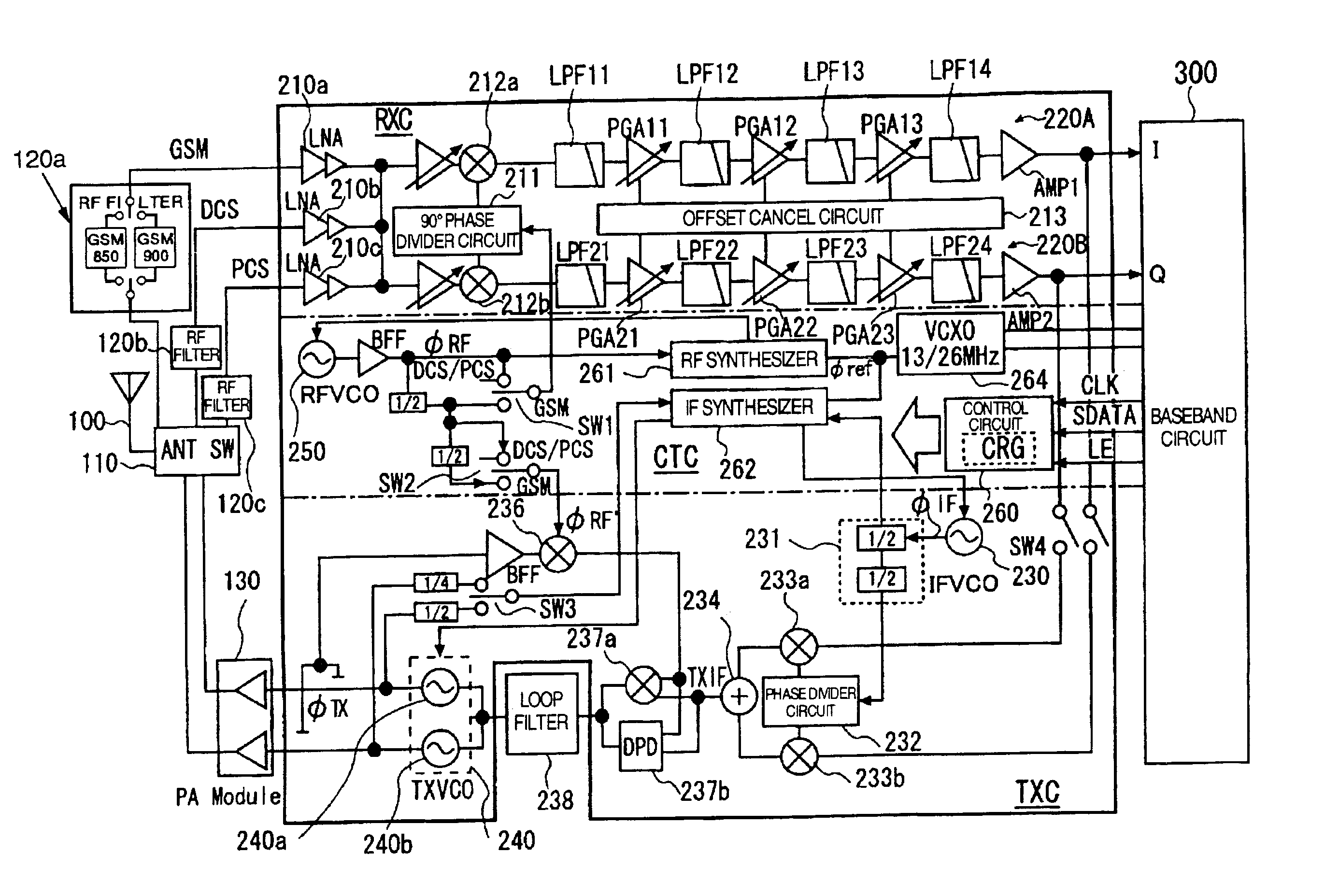
[0032]In the following, one embodiment of the present invention will be described with reference to the accompanying drawings.

[0033]FIG. 1 is a block diagram illustrating an exemplary configuration of a multi-band communication semiconductor integrated circuit (high frequency IC) according to one embodiment of the present invention, and a radio communication system using the communication semiconductor integrated circuit.

[0034]The radio communication system illustrated in FIG. 1 comprises an antenna 100 for transmitting and receiving signal radio waves; a switch 110 for switching transmission and reception; high frequency filters 120a-120c such as SAW filters for removing unwanted waves from a reception signal; a high frequency power amplifier 130 for amplifying a transmission signal; a high frequency IC 200 for demodulating a reception signal and modulating a transmission signal; and a baseband circuit (LSI) 300 for converting transmission data to I, Q signals and controlling the h...


PUM


Abstract

A communication semiconductor integrated circuit has an oscillator circuit forming part of a transmission PLL circuit fabricated on a single semiconductor chip together with an oscillator circuit forming part of a reception PLL circuit and an oscillator circuit for an intermediate frequency. The oscillator circuit forming part of the transmission PLL circuit is configured to be operable in a plurality of bands. A circuit for measuring the oscillating frequency of the oscillator circuit forming part of the transmission PLL circuit is also used for measuring the oscillating frequency of the oscillator circuit forming part of the reception PLL circuit or for measuring the oscillating frequency of the oscillator circuit for the intermediate frequency.

Description

CROSS-REFERENCE TO RELATED APPLICATION[0001]The present application relates to subject matters described in the U.S. patent applications being file based on the United Kingdom Patent Application No. 0221303.1 filed on May 31, 2002. That U.S. application is assigned to the same assignees of the present application.BACKGROUND OF THE INVENTION[0002]The present invention relates generally to techniques which are effectively applied to an on-chip voltage controlled oscillator circuit (VCO) that can switch oscillating frequencies, and more particularly, to techniques which are effectively utilized in high frequency semiconductor integrated circuits and radio communication systems for demodulating a reception signal and modulating a transmission signal in radio communication apparatuses, for example, a portable telephone and the like which can transmit and receive signals in a plurality of bands.[0003]A radio communication system such as a portable telephone uses a PLL (phase locked loop) ...

Claims


Application Information

Patent Timeline
IPC IPC(8): H03D3/00H03J1/00H03L7/089H03J7/02H03L7/08H03L7/10H03J7/06H03L7/193H03L7/16H03L7/18H03L7/187H04B1/40
CPCH03D3/008H03J1/005H03L7/193H03L7/0891H03L7/10H03J7/06H03L7/103H03L7/18H04B1/406
Inventor OOSAWA, HIROTAKASHINBO, JIROKURAKAMI, NORIYUKIKASAHARA, MASUMIHENSHAW, ROBERT ASTLE
Owner RENESAS ELECTRONICS CORP
Why Eureka
Try Eureka