High frequency power amplifier circuit and radio communication system

a power amplifier circuit and high frequency technology, applied in the direction of automatic tone/bandwidth control, gain control, sustainable buildings, etc., can solve the problems of power loss in the coupler, reduced packaging density, and increased circuit size, and achieve high packaging density, high power efficiency, and high frequency power amplifier circuit

Inactive Publication Date: 2006-10-17
RENESAS TECH CORP
View PDF7 Cites 20 Cited by
  • Summary
  • Abstract
  • Description
  • Claims
  • Application Information

AI Technical Summary

Benefits of technology

[0010]The abovementioned closed loop system, which controls output power by controlling gate bias voltages by the APC circuit, is advantageous in that power efficiency is satisfactory regardless of whether an output level is low or high. However, there is a disadvantage with the closed loop system in that, since it requires a coupler and the APC circuit, the circuit size increases and packaging density decreases, and power losses occur in the coupler.
[0011]On the other hand, the high frequency power amplifier circuit of the abovementioned power voltage control system advantageously has high packaging density and low power losses because it requires no coupler. However, in the invention proposed previously, power voltages are supplied from a transistor for power voltage control common to the amplifying stages, and with a gate bias voltage fixed, the power voltages are changed to control output power.

Problems solved by technology

However, there is a disadvantage with the closed loop system in that, since it requires a coupler and the APC circuit, the circuit size increases and packaging density decreases, and power losses occur in the coupler.
As a result, the following problems have become apparent.
That is, an attempt to increase power efficiency with a gate bias voltage kept low causes lack of output power in high regions of demanded output power, failing to obtain a desired output level.
On the other hand, an attempt to obtain sufficient output power with a gate bias voltage kept high produces an excessive amount of current in low regions of demanded output power as shown by a broken line A in FIG. 11, reducing power efficiency.

Method used


Image

  • High frequency power amplifier circuit and radio communication system
  • High frequency power amplifier circuit and radio communication system
  • High frequency power amplifier circuit and radio communication system

Examples


first embodiment

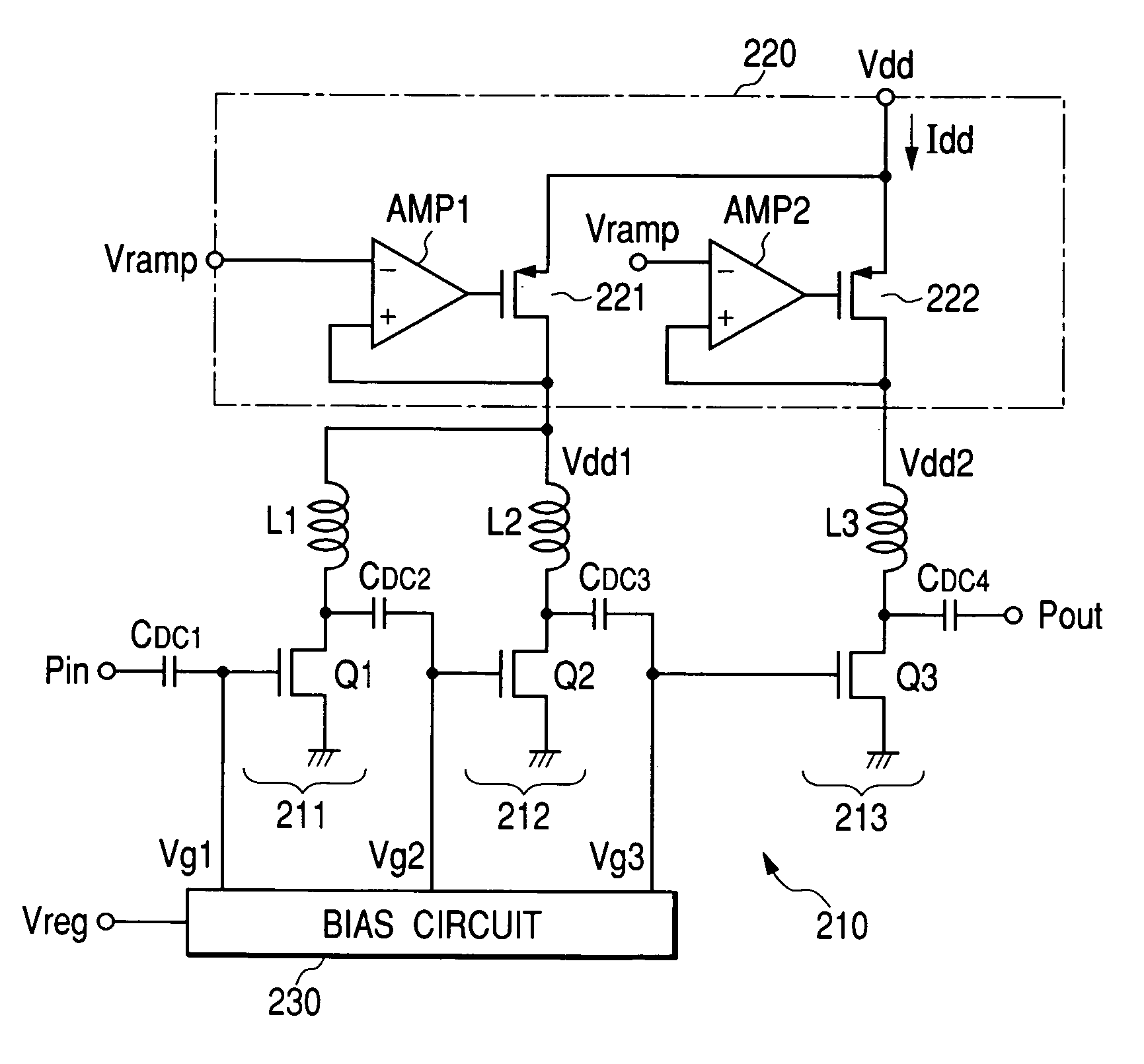
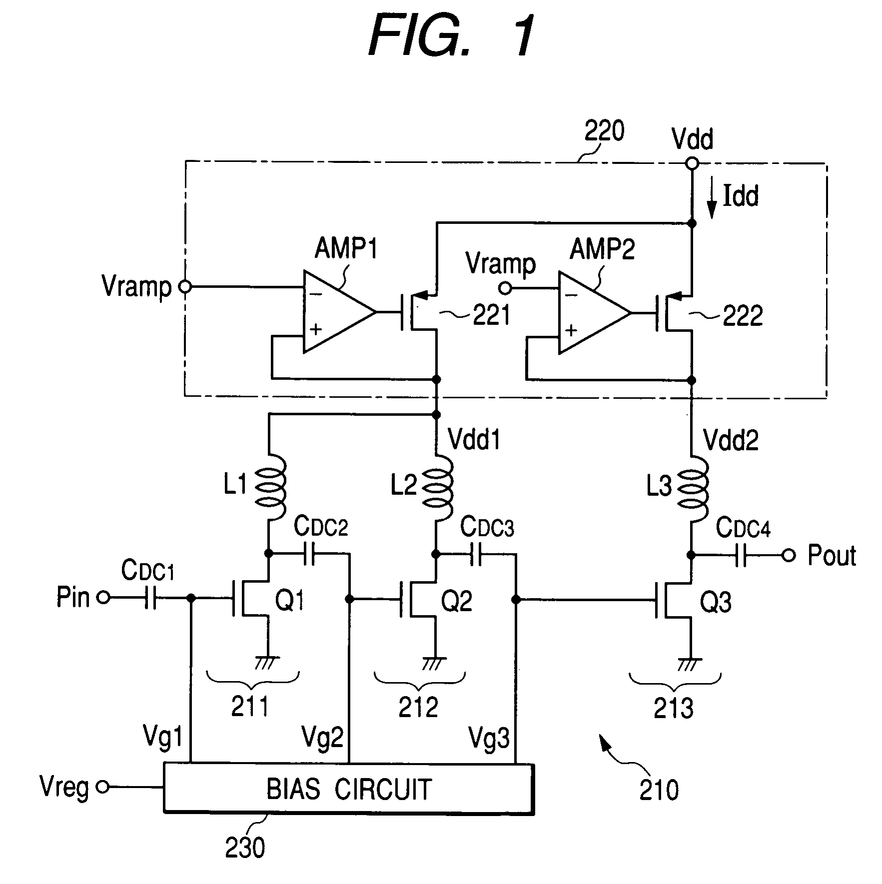
[0035]FIG. 1 shows the outline configuration of a high frequency power amplifier circuit according to the present invention. Though there is no particular limitation, a high frequency power amplifier circuit of this embodiment is formed as a module with plural semiconductor chips and discrete parts such as capacitances mounted on an insulating substrate such as a ceramic substrate.

[0036]The high frequency power amplifier circuit of the embodiment of FIG. 1 (RF power module) comprises a power amplifier 210 comprising three amplifying stages 211, 212, and 213, a power voltage control circuit 220 controlling a voltage applied to a power voltage terminal of the power amplifier 210, and a bias circuit 230 applying bias voltages Vg1, Vg2, and Vg3 to the amplifying stages 211, 212, and 213. The bias circuit 230 can be comprised of, for example, a resistive voltage divider that generates voltages Vg1, Vg2, and Vg3 by dividing a voltage Vreg supplied from a baseband circuit or the like (not ...

second embodiment

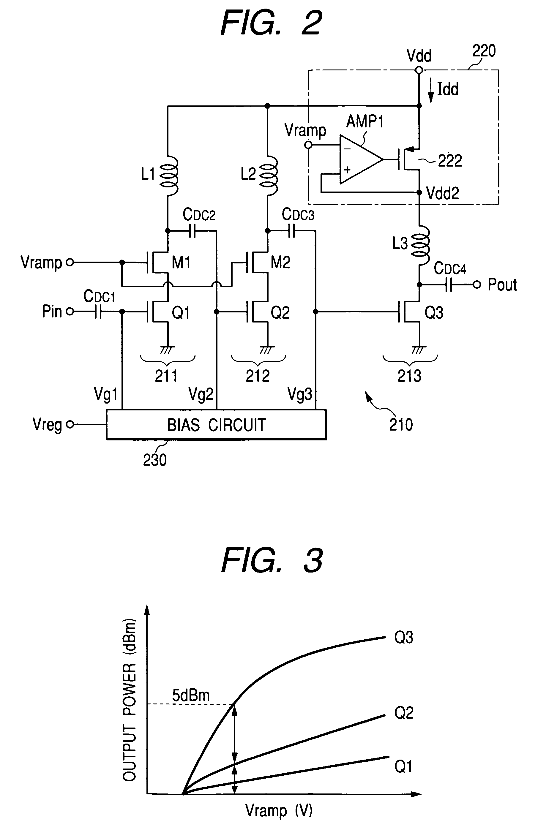
[0047]FIG. 2 shows a high frequency power amplifier circuit to which the present invention is applied. In a power amplifier 210 of the high frequency power amplifier circuit of this embodiment, first and second amplifying stages 211 and 212 of three amplifying stages 211, 212, and 213 respectively comprise FETs Q1 and Q2 for amplification and MOSFETs M1 and M2 connected in series with the FETs, an output level specification signal Vramp being applied to gate terminals of the MOSFETs M1 and M2. The three-stage amplifying stage 213 comprises only an FET Q3 for amplification.

[0048]The power voltage control circuit 220, provided with only the third amplifying stage 213, comprises a transistor 222 for power voltage control, configured by a P-channel MOSFET, connected between a power voltage terminal Vdd and a drain terminal of a FET Q3 for amplification of the third amplifying stage 213, and an operational amplifier AMP2 connected to a gate terminal of the transistor 222.

[0049]FETs Q1, Q...


PUM


Abstract

Providing a high frequency power amplifier circuit and a radio communication system which can control output power by a power voltage, produce sufficient output power in high regions of demanded output power and improve power efficiency in low regions of demanded output power. In a high frequency power amplifier circuit (RF power module) which comprises two or more cascaded FETs for amplification and controls output power by controlling power voltages of the FETs for amplification to gate terminals of which bias voltages of a predetermined level are applied, different transistors for power voltage control are provided for a last-stage FET for amplification and preceding-stage FETs for amplification. The transistors for power voltage control generate and apply the power voltage so that the preceding-stage FETs for amplification saturate when a demanded output level is relatively low.

Description

CROSS-REFERENCE TO RELATED APPLICATION[0001]The present application claims priority from Japanese patent application JP 2003-183696 filed on Jun. 27, 2003, the content of which is hereby incorporated by reference into this application.BACKGROUND OF THE INVENTION[0002]The present invention relates to a technique effectively applied to a high frequency power amplifier circuit and a radio communication device such as a cellular phone incorporating the high frequency power amplifier circuit, and more particularly to a technique for improving an output power level and power efficiency in a high frequency power amplifier circuit capable of controlling the power voltages of amplification transistors making up the high frequency power amplifier circuit to control output power.[0003]A high frequency power amplifier circuit (in general, configured in multiple stages) that uses semiconductor amplifying elements such as MOS FET (Field Effect Transistor) and GaAs-MESFET is built into an output p...

Claims


Application Information

Patent Timeline
Patent Type & Authority Patents(United States)
IPC IPC(8): H03G3/30H03F3/21H03F1/02H04B1/04
CPCH03F1/0211H03G3/3047H03F2200/408Y02B60/50
Inventor TAHARA, KENJITSUTSUI, TAKAYUKIADACHI, TETSUAKI
Owner RENESAS TECH CORP
Why Eureka
Try Eureka